ST13005
STB13005-1
HIGH VOLTAGE FAST-SWITCHING
NPN POWER TRANSISTORS
s
MEDIUM VOLTAGE CAPABILITY
s
NPN TRANSISTORS
s
LOW SPREAD OF DYNAMIC PARAMETERS
s
MINIMUM LOT-TO-LOT SPREAD FOR
RELIABLE OPERATION
s
VERY HIGH SWITCHING SPEED
s
THROUGH-HOLE I2PAK (TO-262) POWER
PACKAGE IN TUBE (SUFFIX "-1")
APPLICATIONS:
s
ELECTRONIC BALLASTS FOR
FLUORESCENT LIGHTING
s
SWITCH MODE POWER SUPPLIES
DESCRIPTION
The devices are is manufactured using high
voltage Multi Epitaxial Planar technology for high
switching speeds and medium voltage capability.
They use a Cellular Emitter structure with planar
edge termination to enhance switching speeds
while maintaining the wide RBSOA.
Æ
INTERNAL SCHEMATIC DIAGRAM
January 1999
ABSOLUTE MAXIMUM RATINGS
Symbol
Parameter
Val ue
Uni t
V
CES
Collector-Emit ter Volt age (V
BE
= 0)
700
V
V
CEO
Collector-Emit ter Volt age (I
B
= 0)
400
V
V
EBO
Emitt er-Base Voltage (I
C
= 0)
9
V
I
C
Collector Current
4
A
I
CM
Collector Peak Current (t
p
< 5 ms)
8
A
I
B
Base Current
2
A
I
BM
Base Peak Current (t
p
< 5 ms)
4
A
P
t ot
Tot al Dissipation at T
c
= 25
o
C
75
W
T
stg
St orage Temperature
-65 to 150
o
C
T
j
Max. Operat ing Junction Temperat ure
150
o
C
1 2
3
TO-220
I2PAK
TO-262
(Suffix "-1")
1
2
3
1/8

THERMAL DATA
R
t hj-ca se
Thermal Resistance Junction-case
Max
1.67
o
C/W
ELECTRICAL CHARACTERISTICS (T
case
= 25
o
C unless otherwise specified)
Symb ol
Parameter
Test Cond ition s
Mi n.
Typ .
Max.
Un it
I
CEV
Collector Cut -of f
Current (V
BE
= -1.5V)
V
CE
= 700V
V
CE
= 700V
T
ca se
= 100
o
C
1
5
mA
mA
I
EBO
Emitt er Cut -of f
Current (I
C
= 0)
V
EB
= 9 V
1
mA
V
CEO(sus )
Collector-Emit ter
Sustaining Voltage
(I
B
= 0)
I
C
= 10 mA
400
V
V
CE(sat )
Collector-Emit ter
Saturation Voltage
I
C
= 1 A
I
B
= 0.2 A
I
C
= 2 A
I
B
= 0.5 A
I
C
= 4 A
I
B
= 1 A
0.5
0.6
1
V
V
V
BE(s at)
Base-Emitt er
Saturation Voltage
I
C
= 1 A
I
B
= 0.2 A
I
C
= 2 A
I
B
= 0.5 A
1.2
1.6
V
V
h
FE
DC Current Gain
I
C
= 1 A
V
CE
= 5 V
Group A
Group B
I
C
= 2 A
V
CE
= 5 V
15
27
8
32
45
40
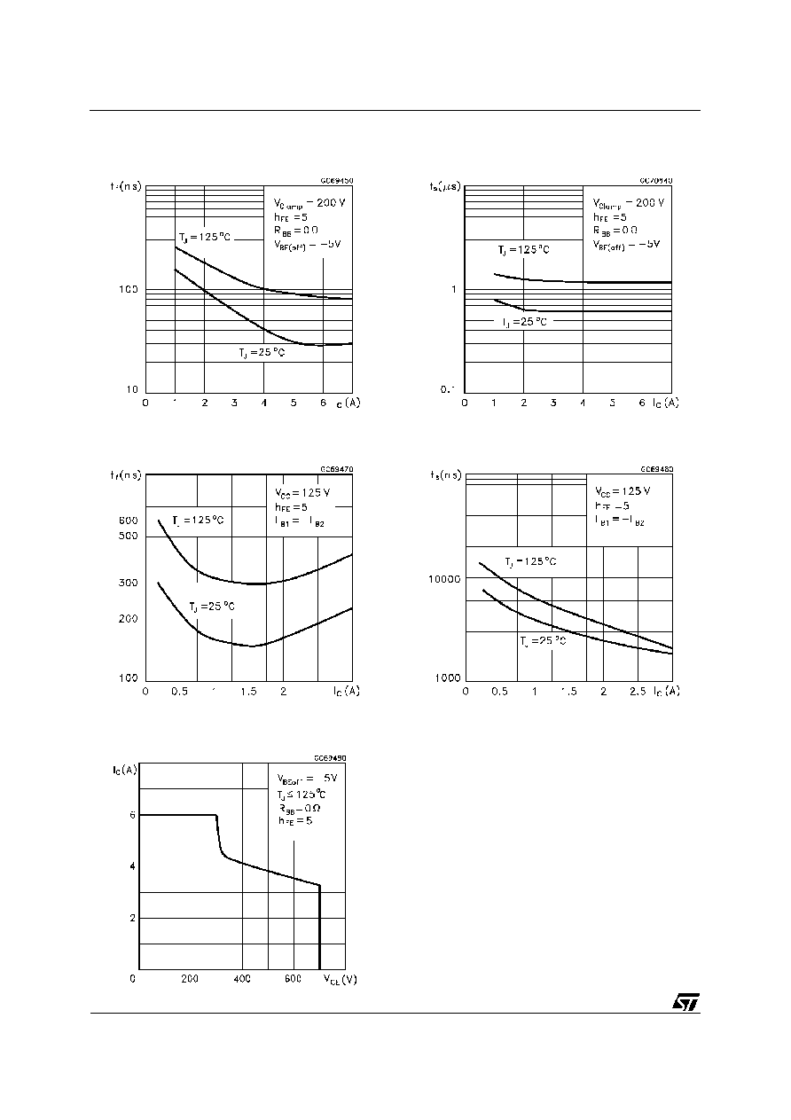
t
s
t
f
RESI STIVE LO AD
St orage Time
Fall Time
I
C
= 2 A
I
B1
= -I
B2
= 0.4 A
V
CC
= 125 V
T
p
= 30
µ
s
1. 5
0.2
3.0
µ
s
µ
s
Pulsed: Pulse duration = 300
µ
s, duty cycle = 1.5 %
Note : Product is pre-selected in DC current gain (GROUP A and GROUP B). STMicroelectronics reserves the right to ship either groups
according to production availability. Please contact your nearest STMicroelectronics sales office for delivery details.
ST13005 / STB13005-1
2/8

Figure 1: Inductive Load Switching Test Circuit.
Figure 2: Resistive Load Switching Test Circuit.
1) Fast elect ronic switch
2) Non-induct ive Resistor
3) Fast recovery rectif ier
1) Fast elect ronic switch
2) Non-induct ive Resistor
ST13005 / STB13005-1
5/8