 | –≠–ª–µ–∫—Ç—Ä–æ–Ω–Ω—ã–π –∫–æ–º–ø–æ–Ω–µ–Ω—Ç: ST13007D | –°–∫–∞—á–∞—Ç—å:  PDF PDF  ZIP ZIP |

ST13007D
HIGH VOLTAGE FAST-SWITCHING
NPN POWER TRANSISTOR
s
IMPROVED SPECIFICATION:
- LOWER LEAKAGE CURRENT
- TIGHTER GAIN RANGE
- DC CURRENT GAIN PRESELECTION
- TIGHTER STORAGE TIME RANGE
s
HIGH VOLTAGE CAPABILITY
s
INTEGRATED FREE-WHEELING DIODE
s
LOW SPREAD OF DYNAMIC PARAMETERS
s
MINIMUM LOT-TO-LOT SPREAD FOR
RELIABLE OPERATION
s
VERY HIGH SWITCHING SPEED
s
FULLY CHARACTERIZED AT 125
o
C
s
LARGE RBSOA
APPLICATIONS
s
UP TO 120W ELECTRONIC
TRANSFORMERS FOR HALOGEN LAMPS
s
SWITCH MODE POWER SUPPLIES
DESCRIPTION
The device is manufactured using high voltage
Multi Epitaxial Planar technology for high
switching speeds and high voltage capability.
It uses a Cellular Emitter structure to enhance
switching speeds.
INTERNAL SCHEMATIC DIAGRAM
April 2003
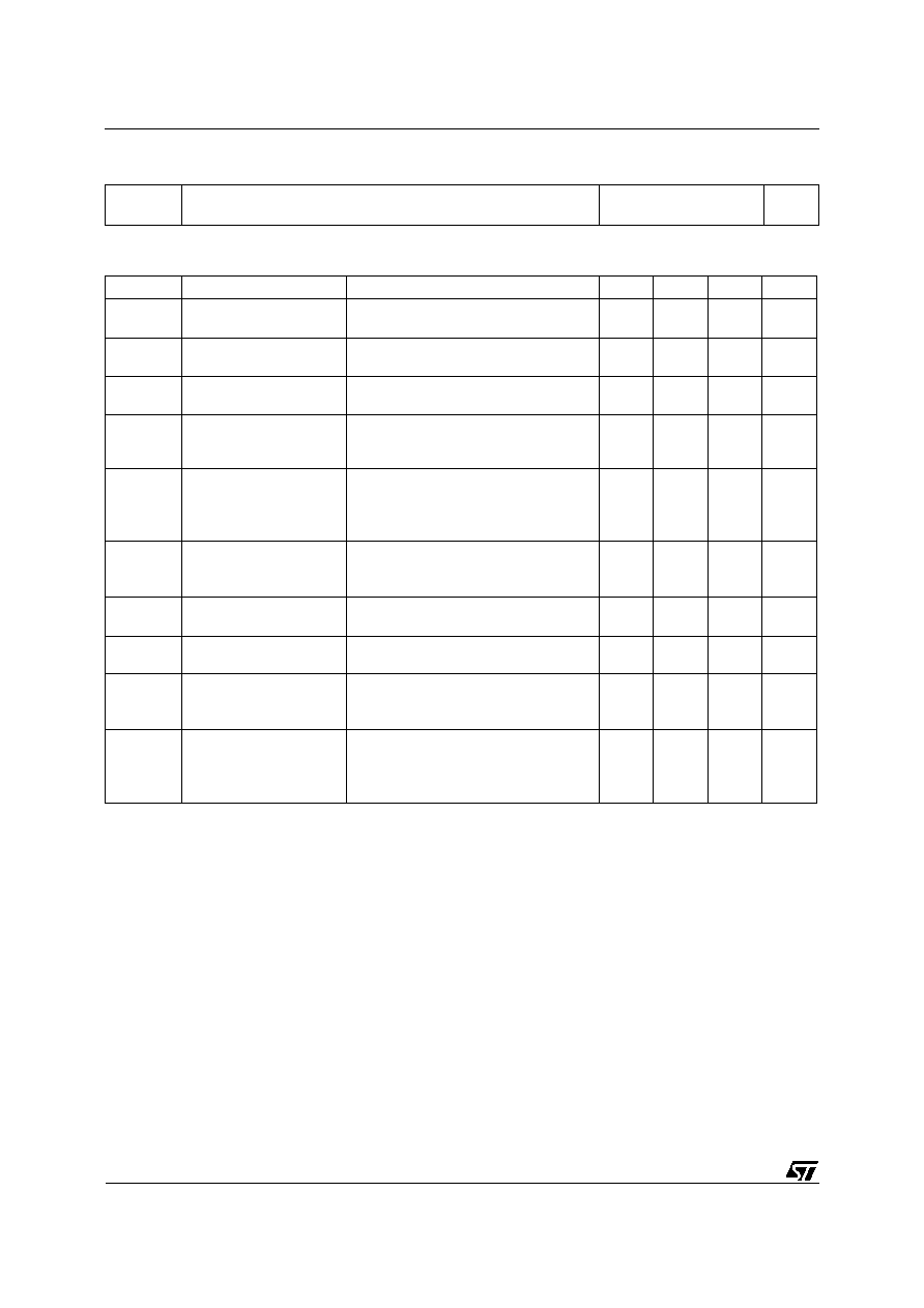
ABSOLUTE MAXIMUM RATINGS
Symbol
Parameter
Value
Unit
V
CEV
Collector-Emitter Voltage (V
BE
= -1.5V)
700
V
V
CEO
Collector-Emitter Voltage (I
B
= 0)
400
V
V
EBO
Emitter-Base Voltage (I
C
= 0)
9
V
I
C
Collector Current
8
A
I
CM
Collector Peak Current
16
A
I
B
Base Current
4
A
I
BM
Base Peak Current
8
A
P
tot
Total Dissipation at T
c
25
o
C
80
W
T
stg
Storage Temperature
-65 to 150
o
C
T
j
Max. Operating Junction Temperature
150
o
C
1
2
3
TO-220
Æ
1/7
THERMAL DATA
R
thj-case
R
thj-amb
Thermal Resistance Junction-case Max
Thermal Resistance Junction-ambient Max
1.56
62.5
o
C/W
o
C/W
ELECTRICAL CHARACTERISTICS (T
case
= 25
o
C unless otherwise specified)
Symbol
Parameter
Test Conditions
Min.
Typ.
Max.
Unit
I
CES
Collector Cut-off
Current (V
BE
= 0)
V
CE
= 700 V
V
CE
= 700 V T
c
= 100
o
C
10
0.5
µ
A
mA
I
CEO
Collector Cut-off
Current (I
B
= 0)
V
CE
= 400 V
100
µ
A
I
EBO
Emitter Cut-off Current
(I
C
= 0)
V
EB
= 9 V
100
µ
A
V
CEO(sus)
Collector-Emitter
Sustaining Voltage
(I
B
= 0)
I
C
= 10 mA
400
V
V
CE(sat)
Collector-Emitter
Saturation Voltage
I
C
= 2 A I
B
= 0.4 A
I
C
= 5 A I
B
= 1 A
I
C
= 8 A I
B
= 2 A
I
C
= 5 A I
B
= 1 A T
c
= 100
o
C
0.8
1.5
2
3
V
V
V
V
V
BE(sat)
Base-Emitter
Saturation Voltage
I
C
= 2 A I
B
= 0.4 A
I
C
= 5 A I
B
= 1 A
I
C
= 5 A I
B
= 1 A T
c
= 100
o
C
1.2
1.6
1.5
V
V
V
h
FE
DC Current Gain
I
C
= 2 A V
CE
= 5 V
I
C
= 5 A V
CE
= 5 V
18
8
40
25
V
f
Diode Forward
Voltage
I
C
= 3 A
2.5
V
t
s
t
f
INDUCTIVE LOAD
Storage Time
Fall Time
I
C
= 5 A V
CL
= 250 V R
BB
= 0
I
B1
= 1 A V
BE(off)
= -5 V
L = 200
µ
H (see figure 1)
1.7
90
2.3
150
µ
s
ns
t
s
t
f
INDUCTIVE LOAD
Storage Time
Fall Time
I
C
= 5 A V
CL
= 250 V R
BB
= 0
B1
= 1 A V
BE(off)
= -5 V
L = 200
µ
H T
C
= 125
o
C
(see figure 1)
2.2
150
µ
s
ns
* Pulsed: Pulse duration = 300
µ
s, duty cycle 2 %.
ST13007D
2/7

Safe Operating Area
DC Current Gain
Collector Emitter Saturation Voltage
Derating Curve
DC Current Gain
Base Emitter Saturation Voltage
ST13007D
3/7

Diode Forward Voltage
Switching Time Inductive Load
Switching Time Resistive Load
Reverse Biased SOA
ST13007D
4/7

Figure 1: Inductive Load Switching Test Circuit.
Figure 2: Resistive Load Switching Test Circuit.
1) Fast electronic switch
2) Non-inductive Resistor
3) Fast recovery rectifier
1) Fast electronic switch
2) Non-inductive Resistor
ST13007D
5/7