
1/9
January 2002
s
SINGLE +5v SUPPLY OPERATION
s
0.1
µ
F EXTENAL CHARGE PUMP
CAPACITORS
s
500kbps DATE RATE UNDER LOAD
s
LOWER SUPPLY CURRENT 1.5mA (TYP)
s
IDEAL FOR HIGH SPEED RS-232
APPLICATIONS
s
PACKAGED IN SO-24, SSO-24 AND
TSSOP24
s
ESD PROTECTION FOR RS-232 I/O PINS:
±
15 KV HUMAN BODY MODEL
DESCRIPTION
The ST207EH is a high speed enhanced
multi-channel RS-232 line transceivers with
improved electrical performance. The ST207EH is
a superior drop-in replacement to our previous
versions as well as popular industry standards.
The device feature low-power CMOS construction
and the charge pump circuitry that generates the
±
10V RS-232 voltag elevels using 01
µ
F charges
pump capacitors. The ST207EH include a high
transmission rate of 500Kbps, a lower supply
current at 1.5mA typical (no load), and a superior
ESD performance. The ESD tolerance has been
improved for this device over ±15KV for HUMAN
Body Model. The ST207EH cames in 24-pin SO,
SSO and TSSOP packages.
ORDERING CODES
Type
Temperature
Range
Package
Comments
ST207EHCD
0 to 70 ∞C
SO-24 (Tube)
33parts per tube / 25tube per box
ST207EHBD
-40 to 85 ∞C
SO-24 (Tube)
33parts per tube / 25tube per box
ST207EHCDR
0 to 70 ∞C
SO-24 (Tape & Reel)
1000 parts per reel
ST207EHBDR
-40 to 85 ∞C
SO-24 (Tape & Reel)
1000 parts per reel
ST207EHCPR
0 to 70 ∞C
SSOP-24 (Tape & Reel)
1350 parts per reel
ST207EHBDR
-40 to 85 ∞C
SSOP-24 (Tape & Reel)
1350 parts per reel
ST207EHCTR
0 to 70 ∞C
TSSOP24 (Tape & Reel)
2500 parts per reel
ST207EHBTR
-40 to 85 ∞C
TSSOP24 (Tape & Reel)
2500 parts per reel
ST207EH
±
15KV ESD PROTECTED
5V HIGH PERFORMANCE RS-232 TRANSCEIVER
SSOP
SOP
TSSOP

ST207EH
2/9
PIN CONFIGURATION
PIN DESCRIPTION
PlN N∞
SYMBOL
NAME AND FUNCTION
1
T3
OUT
RS-232 Driver Output
2
T1
OUT
RS-232 Driver Output
3
T2
OUT
RS-232 Driver Output
4
R1
IN
RS-232 Receiver Input
5
R1
OUT
TTL/CMOS Receiver Output
6
T2
IN
TTL/CMOS Driver Input Internal Pull-up to V
CC
7
T1
IN
TTL/CMOS Driver Input Internal Pull-up to V
CC
8
GND
Ground
9
V
CC
4.75V to 5.25V Supply Voltage
10
C
1+
Terminal For Positive Charge-pump Capacitor
11
V
+
2V
CC
Generated by The Charge-pump
12
C
1-
Terminal For Negative Charge-pump Capacitor
13
C
2+
Terminal For Positive Charge-pump Capacitor
14
C
2-
Terminal For Negative Charge-pump Capacitor
15
V
-
-2V
CC
Generated by The Charge-pump
16
R3
IN
RS-232 Receiver Input
17
R3
OUT
TTL/CMOS Receiver Output
18
T3
IN
TTL/CMOS Driver Input Internal Pull-up to V
CC
19
T4
IN
TTL/CMOS Driver Input Internal Pull-up to V
CC
20
T5
OUT
RS-232 Driver Output
21
T5
IN
TTL/CMOS Driver Input Internal Pull-up to V
CC
22
R2
OUT
TTL/CMOS Receiver Output
23
R2
IN
RS-232 Receiver Input
24
T4
OUT
RS-232 Driver Output
ST207EH
3/9
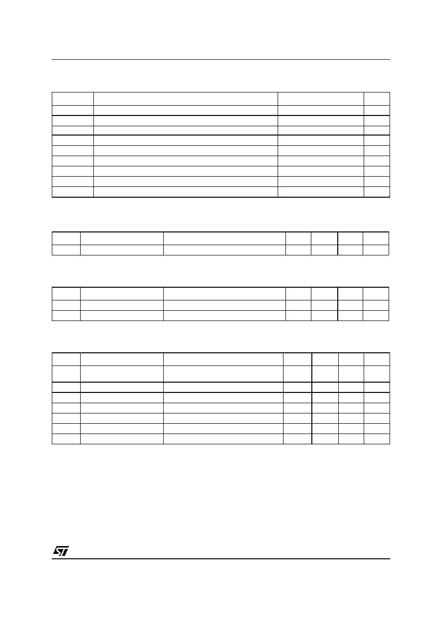
ABSOLUTE MAXIMUM RATINGS
Absolute Maximum Ratings are those values beyond which damage to the device may occur. Functional operation under these condition is
not implied. V+ and V- can have a maximum magnitude of +7V, but their absolute addition can not exceed 13 V.
ESD PERFORMANCE: TRANSMITTER OUTPUTS, RECEIVER INPUTS
ELECTRICAL CHARACTERISTICS (C
1
- C
4
= 0.1
µ
F, V
CC
= 5V
±
5%, T
A
= MIN to MAX, unless
otherwise specified. Typical values are referred to T
A
= 25∞C)
RECEIVER ELECTRICAL CHARACTERISTICS (C
1
- C
4
= 0.1
µ
F, V
CC
= 5V
±
5%, T
A
= MIN to MAX,
unless otherwise specified. Typical values are referred to T
A
= 25∞C)
Symbol
Parameter
Value
Unit
V
CC
Supply Voltage
6
V
V+
Extra Positive Voltage
(V
CC
- 0.3) to 13.2
V
V-
Extra Negative Voltage
13.2
V
T
IN
Transmitter Input Voltage Range
-0.3 to (V
CC
+ 0.3)
V
R
IN
Receiver Input Voltage Range
±
20
V
T
OUT
Transmitter Output Voltage Range
(V- - 0.3) to (V+ + 0.3)
V
R
OUT
Receiver Output Voltage Range
-0.3 to (V
CC
+ 0.3)
V
T
SHORT
Short Circuit Durtion on T
OUT
Continuous
T
stg
Storage Temperature Range
-65 to 150
∞C
Symbol
Parameter
Test Conditions
Min.
Typ.
Max.
Unit
ESD
ESD Protection Voltage
Human Body Model
±
15
KV
Symbol
Parameter
Test Conditions
Min.
Typ.
Max.
Unit
V
CC
Supply Voltage
4.5
5.0
5.5
V
I
CC
V
CC
Power Supply Current
No Load T
A
= 25∞C` V
CC
=
±
10%
1.5
3
mA
Symbol
Parameter
Test Conditions
Min.
Typ.
Max.
Unit
V
RIN
Receiver Input Voltage
Operating Range
-15
15
V
V
RIL
Input Threshold Low
T
A
= 25∞C
V
CC
= 5V
0.8
1.2
V
V
RIH
Input hreshold High
T
A
= 25∞C
V
CC
= 5V
1.7
2.8
V
V
RIHYS
Input Hysteresys
V
CC
= 5V,
0.2
0.5
1
V
R
RIN
Input Resistance
T
A
= 25∞C
V
IN
=
±
15V
3
5
7
K
V
OL
Output Voltage Low
I
OUT
= 3.2mA
V
CC
= 5V
0.4
V
V
OH
Output Voltage High
I
OUT
= -1mA
3.5
V

ST207EH
4/9
TRANSMITTER ELECTRICAL CHARACTERISTICS (C
1
- C
4
= 0.1
µ
F, V
CC
= 5V
±
5%, T
A
= MIN to MAX,
unless otherwise specified. Typical values are referred to T
A
= 25∞C)
TIMING CHARACTERISTICS (C
1
- C
4
= 0.1
µ
F, V
CC
= 5V
±
5%, T
A
= MIN to MAX, unless otherwise
specified. Typical values are referred to T
A
= 25∞C)
Symbol
Parameter
Test Conditions
Min.
Typ.
Max.
Unit
V
TOUT
Output Voltage Swing
All Driver loaded with 3K
to GND
±
5
±
7
V
R
OUT
Transmitter Output
Resistance
V
CC
= V+ = V- = 0V
V
OUT
=
±
2V
300
I
SC
Output Short Circuit Current Infinite duration
V
OUT
= 0V
±
18
mA
I
IL
Input Pull-Up Current
T
IN
= 0V
15
200
µ
A
V
TIL
Input Logic Threshold Low
0.8
V
V
TIH
Input Logic Threshold High
0.2
V
Symbol
Parameter
Test Conditions
Min.
Typ.
Max.
Unit
D
R
Maximum Data Rate
R
L
= 3K
C
L
= 1000pF
480
Kbps
t
PHLR
t
PLHR
Receiver Propagation Delay RS-232 to TTL
250
ns
t
PHLT
t
PLHT
Transmitter Propagation
Delay
TTL to RS-232
200
500
ns

ST207EH
5/9
APPLICATION CIRCUITS
CAPACITANCE VALUE (
µ
F)
C1
C2.
C3
C4
C5
0.1
0.1
0.1
0.1
0.1

ST207EH
6/9
DIM.
mm.
inch
MIN.
TYP
MAX.
MIN.
TYP.
MAX.
A
2.65
0.104
a1
0.1
0.2
0.004
0.008
a2
2.45
0.096
b
0.35
0.49
0.014
0.019
b1
0.23
0.32
0.009
0.012
C
0.5
0.020
c1
45∞ (typ.)
D
15.20
15.60
0.598
0.614
E
10.00
10.65
0.393
0.419
e
1.27
0.050
e3
13.97
0.550
F
7.40
7.60
0.291
0.300
L
0.50
1.27
0.020
0.050
S
8∞ (max.)
SO-24 MECHANICAL DATA
PO13T
F
C
L
E
a1
b1
A
e
D
e3
b
24
13
1
12
c1
s
a2

ST207EH
7/9
DIM.
mm.
inch
MIN.
TYP
MAX.
MIN.
TYP.
MAX.
A
2
0.079
A1
0.25
0.010
A2
1.51
2.00
0.059
0.079
b
0.25
0.30
0.35
0.010
0.012
0.014
c
0.10
0.35
0.004
0.014
D
8.35
9.35
0.329
0.368
E
7.6
8.7
0.246
0.252
0.256
E1
5.02
6.10
6.22
0.198
0.240
0.245
e
0.65 BSC
0.0256 BSC
K
0∞
10∞
0∞
10∞
L
0.25
0.50
0.80
0.010
0.020
0.031
SSOP24 MECHANICAL DATA
c
E
b
A2
A
E1
D
1
PIN 1 IDENTIFICATION
A1
L
K
e

ST207EH
8/9
DIM.
mm.
inch
MIN.
TYP
MAX.
MIN.
TYP.
MAX.
A
1.1
0.043
A1
0.05
0.15
0.002
0.006
A2
0.9
0.035
b
0.19
0.30
0.0075
0.0118
c
0.09
0.20
0.0035
0.0079
D
7.7
7.9
0.303
0.311
E
6.25
6.5
0.246
0.256
E1
4.3
4.5
0.169
0.177
e
0.65 BSC
0.0256 BSC
K
0∞
8∞
0∞
8∞
L
0.50
0.70
0.020
0.028
TSSOP24 MECHANICAL DATA
c
E
b
A2
A
E1
D
1
PIN 1 IDENTIFICATION
A1
L
K
e
7047476A

ST207EH
9/9
Information furnished is believed to be accurate and reliable. However, STMicroelectronics assumes no responsibility for the
consequences of use of such information nor for any infringement of patents or other rights of third parties which may result from
its use. No license is granted by implication or otherwise under any patent or patent rights of STMicroelectronics. Specifications
mentioned in this publication are subject to change without notice. This publication supersedes and replaces all information
previously supplied. STMicroelectronics products are not authorized for use as critical components in life support devices or
systems without express written approval of STMicroelectronics.
© The ST logo is a registered trademark of STMicroelectronics
© 2002 STMicroelectronics - Printed in Italy - All Rights Reserved
STMicroelectronics GROUP OF COMPANIES
Australia - Brazil - Canada - China - Finland - France - Germany - Hong Kong - India - Israel - Italy - Japan - Malaysia - Malta - Morocco
Singapore - Spain - Sweden - Switzerland - United Kingdom - United States.
© http://www.st.com