 | –≠–ª–µ–∫—Ç—Ä–æ–Ω–Ω—ã–π –∫–æ–º–ø–æ–Ω–µ–Ω—Ç: ST232 | –°–∫–∞—á–∞—Ç—å:  PDF PDF  ZIP ZIP |
ST232
5V POWERED MULTI-CHANNEL
RS-232 DRIVERS AND RECEIVERS
Æ
February 2001
s
SUPPLY VOLTAGE RANGE: 4.5 TO 5.5V
s
SUPPLY CURRENT NO LOAD (TYP): 5mA
s
TRANSMITTER OUTPUT VOLTAGESWING
(TYP):
±
7.8V
s
CONTROLLED OUTPUT SLEW RATE
s
RECEIVER INPUT VOLTAGE RANGE:
±
30V
s
DATA RATE (TYP): 220Kbps
s
OPERATING TEMPERATURE RANGE:
-40 TO 85
o
C, 0 TO 70
o
C
s
COMPATIBLE WITH MAX232 AND MAX202
DESCRIPTION
The ST232 is a 2 driver, 2 receiver device
following EIA/TIA-232 and V.28 communication
standard. It is particularly suitable for applications
where
±
12V is not available. The ST232 uses a
single 5V power supply and only four external
capacitors (0.1
µ
F). Typical applications are in:
Portable
Computers,
Low
Power
Modems,
Interfaces Translation, Battery Powered RS-232
System, Multi-Drop RS-232 Networks.
D
(Micro Package)
N
(Plastic Package)
W
(Micro Package Large)
T
(TSSOP Package)
ORDER CODES
Type
T emperature
Ran ge
Packag e
Comments
ST232CN
0 to 70
o
C
DIP-16
25 parts per tube / 40 tube per box
ST232BN
-40 to 85
o
C
DIP-16
25 parts per tube / 40 tube per box
ST232CD
0 to 70
o
C
SO-16 (Tube)
50 parts per tube / 20 tube per box
ST232BD
-40 to 85
o
C
SO-16 (Tube)
50 parts per tube / 20 tube per box
ST232CDR
0 to 70
o
C
SO-16 (Tape & Reel)
2500 parts per reel
ST232BDR
-40 to 85
o
C
SO-16 (Tape & Reel)
2500 parts per reel
ST232CW
0 to 70
o
C
SO-16 Large (Tube)
49 parts per tube / 25 tube per box
ST232BW
-40 to 85
o
C
SO-16 Large (Tube)
49 parts per tube / 25 tube per box
ST232CWR
0 to 70
o
C
SO-16 Large (Tape & Reel)
1000 parts per reel
ST232BWR
-40 to 85
o
C
SO-16 Large (Tape & Reel)
1000 parts per reel
ST232CT
0 to 70
o
C
TSSOP16 (Tube)
only for samples
ST232BT
-40 to 85
o
C
TSSOP16 (Tube)
only for samples
ST232CTR
0 to 70
o
C
TSSOP16 (Tape & Reel)
2500 parts per reel
ST232BTR
-40 to 85
o
C
TSSOP16 (Tape & Reel)
2500 parts per reel
1/11

PIN CONFIGURATION
PIN DESCRIPTION
PIN No
SYMBOL
NAME AND F UNCTION
1
C
1
+
Positive Terminal for the first Charge Pump Capacitor
2
V+
Doubled Voltage Terminal
3
C
1
-
Negative Terminal for the first Charge Pump Capacitor
4
C
2
+
Positive Terminal for the second Charge Pump Capacitor
5
C
2
-
Negative Terminal for the second Charge Pump Capacitor
6
V-
Inverted Voltage Terminal
7
T2
OUT
Second Transmitter Output Voltage
8
R2
IN
Second Receiver Input Voltage
9
R2
OUT
Second Receiver Output Voltage
10
T2
IN
Second Transmitter Input Voltage
11
T1
IN
First Transmitter Input Voltage
12
R1
OUT
First Receiver Output Voltage
13
R1
IN
First Receiver Input Voltage
14
T1
OUT
First Transmitter Output Voltage
15
GND
Ground
16
V
CC
Supply Voltage
ABSOLUTE MAXIMUM RATINGS (Note 1)
Symbol
Parameter
Val ue
Unit
V
CC
Supply Voltage
-0.3 to 6
V
T
IN
Transmitter Input Voltage Range
-0.3 to (V
CC
+ 0.3)
V
R
IN
Receiver Input Voltage Range
±
30
V
T
OUT
Transmitter Output Voltage Range
(V+ + 0.3) to (V- - 0.3)
V
R
OUT
Receiver Output Voltage Range
-0.3 to (V
CC
+ 0.3)
V
T
SCTOUT
Short Circuit Duration on T
OUT
infinite
T
stg
Storage Temperature Range
-65 to +150
o
C
Absolute Maximum Ratings are those values beyond which damage to the device may occur. Functional operation under these condition is not implied.
Note1: No external supply can be applied toV+ terminal and V- terminal.
ST232
2/11

TRANSMITTER ELECTRICAL CHARACTERISTICS
(C
1
-C
4
= 0.1
µ
F, V
CC
= 5V
±
10%, T
A
= -40 to 85
o
C, unless otherwise specified.
Typical Valus are referred to T
A
= 25
o
C)
Symb ol
Parameter
T est Cond it ion s
Value
Un it
Min.
T yp.
Max.
V
TOUT
Output Voltage Swing
All Transmitter outputs are
loaded with 3K
to GND
±
5
±
7.8
V
I
TIL
Logic Pull-Up Current
T
IN
= 0 V
15
200
µ
A
V
TIL
Input Logic Threshold Low
0.8
V
V
TIH
Input Logic Threshold High
2
V
SR
T
Transition Slew Rate
T
A
= 25
o
C, V
CC
= 5 V,
R
L
= 3 to 7 K
,
C
L
= 50 to 2500 pF (Note 1)
7
30
V/
µ
s
D
R
Data Rate
(Note 2)
120
220
Kbits/s
R
TOUT
Transmitter Output Resistance
V
CC
= V+ = V- = 0V
V
OUT
=
±
2 V
300
I
SC
Transmitter Output Short Circuit
Current
one T
XOUT
to GND
±
10
±
60
mA
Note 1: Measured from 3V to -3Vor from -3V to 3V.
Note 2: One trasmitter output is loaded with R
L
= 3K
to7K
, C
L
= 50 to 1000pF
ELECTRICAL CHARACTERISTICS
(C
1
-C
4
= 0.1
µ
F, V
CC
= 5V
±
10% T
A
= -40 to 85
o
C, unless otherwise specified.
Typical Valus are referred to T
A
= 25
o
C)
Symb ol
Parameter
T est Cond it ion s
Value
Un it
Min.
T yp.
Max.
I
SUPPLY
V
CC
Power Supply Current
No Load,
T
A
= 25
o
C
5
10
mA
RECEIVER ELECTRICAL CHARACTERISTICS
(C
1
-C
4
= 0.1
µ
F, V
CC
= 5V
±
10%, T
A
= -40 to 85
o
C, unless otherwise specified.
Typical Valus are referred to T
A
= 25
o
C)
Symb ol
Parameter
T est Cond it ion s
Value
Un it
Min.
T yp.
Max.
V
RIN
Receiver Input Voltage Operating
Range
-30
30
V
R
RIN
RS-232 Input Resistance
T
A
= 25
o
C, V
CC
= 5 V,
V
RIN
= 5 V
3
5
7
K
V
RIL
RS-232 Input Logic Threshold Low
T
A
= 25
o
C, V
CC
= 5 V
0.8
1.2
V
V
RIH
RS-232 Input Logic Threshold High
T
A
= 25
o
C, V
CC
= 5 V
1.7
2.4
V
V
RIHYS
RS-232 Input Hysteresis
V
CC
= 5 V
0.2
0.5
1
V
V
ROL
TTL/CMOS Output Voltage Low
I
OUT
= 3.2mA (to V
CC
)
0.4
V
V
ROH
TTL/CMOS Output Voltage High
I
OUT
= 1mA (to GND)
3.5
V
CC
-0.4
V
t
dR
Propagation Delay Time
C
L
=150pF (Note 1)
0.3
1
µ
s
I
SCR
Receiver Output Short Circuit Current
±
10
mA
Note 1: RS-232 IN to TTL-CMOS OUT (from 50% to 50%)
ST232
3/11
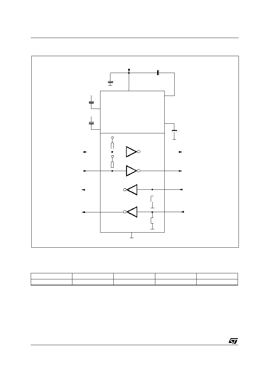
APPLICATION CIRCUITS (note 1, note 2)
C4
+
C1
+
C1+
C1-
3
C2
+
C2+
C2-
4
5
11
10
12
9
TTL / CMOS OUTPUTS
TTL / CMOS INPUTS
V-
6
C5
+
+
C3
+5V INPUT
1
16
Vcc
V+
2
+10V
-10V
RS 232 OUTPUTS
RS 232 INPUTS
14
7
13
8
15
GND
5K
5K
+5V TO +10V
VOLTAGE
DOUBLER
+10V TO -10V
VOLTAGE
INVERTER
+5V
400K
T1
OUT
T1
IN
+5V
400K
T2
IN
T2
OUT
T1
T2
R2
IN
R1
IN
R2
OUT
R1
OUT
R1
R2
Capacitance Value (
µ
F)
C1
C2
C3
C4
C5
0.1
0.1
0.1
0.1
0.1
Note 1: C
1-4
capacitors can even be 1
µ
F ones.
Note 2: C
1-4
canbe common or biased capacitors.
ST232
4/11
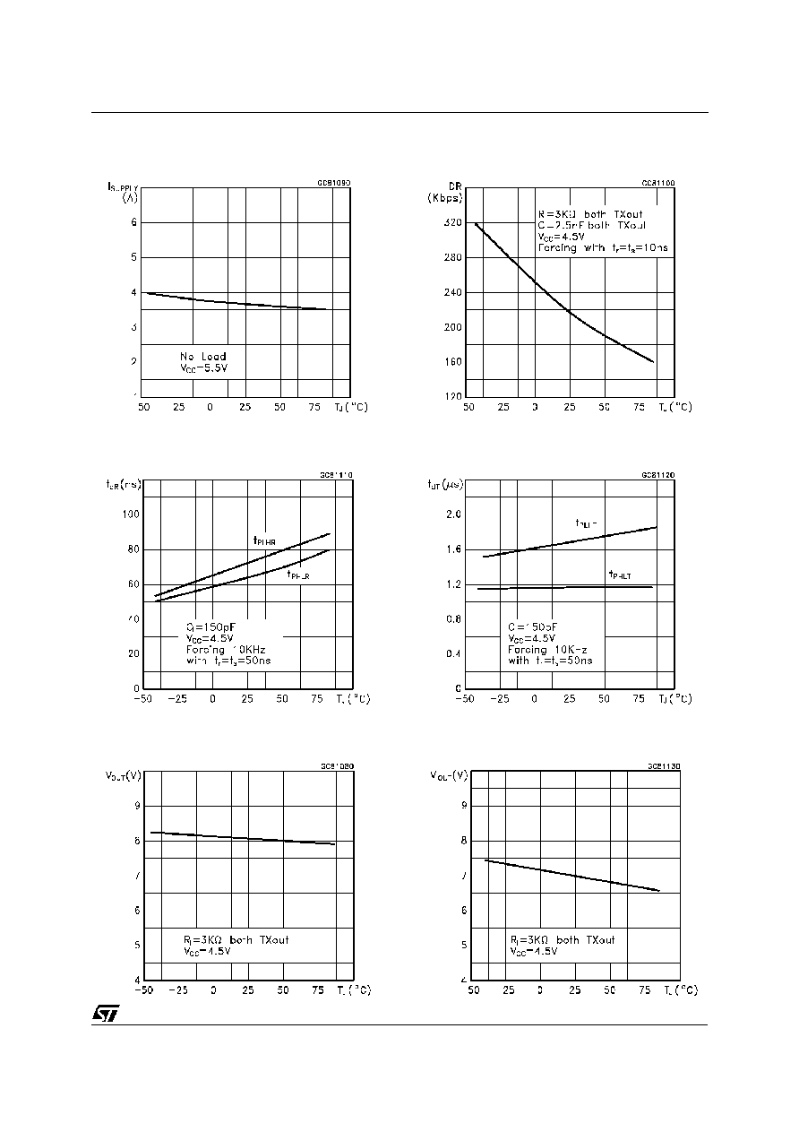
Supply Current vs Temperature
Receiver Propagation Delay
High Level Output Voltage Swing vs Temperature
Data Rate vs Temperature
Driver Propagation Delay
Low Level Output Voltage Swing vs Temperature
ST232
5/11