1/10
December 2002
s
TTL INPUT COMPATIBLE
s
TYPICAL PROPAGATION DELAY: 6ns
s
TYPICAL OUTPUT SKEW: 0.5ns
s
OUTPUT WILL NOT LOAD LINE WHEN
V
CC
=0V
s
MEETS THE REQUIREMENTS OF EIA
STANDARD RS-422
s
OPERATION FROM SINGLE 5V SUPPLY
s
3-STATE OUTPUTS FOR CONNECTION TO
SYSTEM BUSES
s
LOW QUIESCENT CURRENT
s
AVAILABLE IN SURFACE MOUNT
DESCRIPTION
The ST26C31 is a quad differential line driver
designed
for
digital
data
transmission
over
balanced lines and meets all the requirements of
EIA standard RS-422 while retaining the low
power characteristics of CMOS.
The ST26C31 accepts TTL or CMOS input levels
and translates these to RS-422 output levels. This
part uses special outputs circuitry common to all
four drivers. All outputs are protected against
damage due to electrostatic discharge by diode to
VCC and ground.
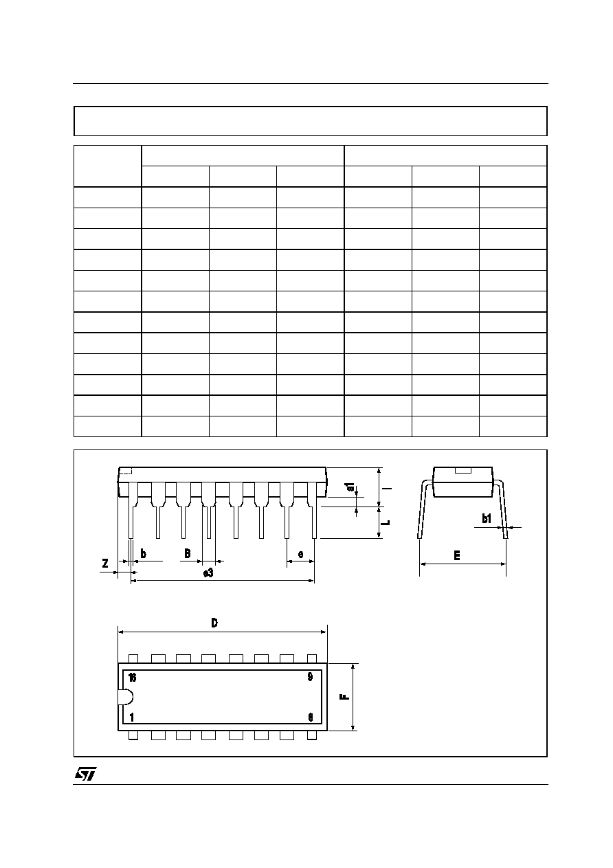
ORDERING CODES
Type
Temperature
Range
Package
Comments
ST26C31BN
-40 to 85 �C
DIP-16
25 parts per tube / 40 tube per box
ST26C31BD
-40 to 85 �C
SO-16 (Tube)
50 parts per tube / 20 tube per box
ST26C31BDR
-40 to 85 �C
SO-16 (Tape & Reel)
2500 parts per reel
ST26C31BTR
-40 to 85 �C
TSSOP16 (Tape & Reel)
2500 parts per reel
ST26C31
CMOS QUAD TRI-STATE
DIFFERENTIAL LINE DRIVER
DIP
SOP
TSSOP

ST26C31
3/10
ABSOLUTE MAXIMUM RATINGS (Note 1, 2)
Note 1: Absolute Maximum Ratings are those values beyond which the safety of the device cannot be guaranteed. They are not meant to
imply that the device should be operated at these limits. The table of electrical characteristics provide conditions for actual device operation.
Note 2: Unless otherwise specified, all voltage are referenced to ground. All currents into the device pins are positive; all currents out of the
device pins are negative.
RECOMMENDED OPERATING CONDITIONS
Symbol
Parameter
Value
Unit
V
CC
Supply Voltage
-0.5 to 7
V
V
IN
DC Input Voltage
-0.5 to (V
CC
+ 0.5)
V
V
OUT
DC Output Voltage (High or Low State)
-0.5 to 7
V
I
IK
Clamp Diode Current
�
20
mA
I
OUT
DC Output Current per Pin
�
150
mA
I
CC
DC V
CC
or GND Current
�
150
mA
T
stg
Storage Temperature Range
-65 to +150
�C
Symbol
Parameter
Value
Unit
V
CC
Supply Voltage
4.5 to 5.5
V
V
IN
DC Input Voltage
0 to V
CC
V
V
OUT
DC Output Voltage (High or Low State)
0 to V
CC
V
V
OUT
DC Output Voltage (V
CC
= 0V or High Impedance)
0 to 5
V
T
A
Operating Temperature Range
-40 to +85
�C
t
r
, t
f
Maximum Enable Input Rise or Fall Times
500
ns
ST26C31
4/10
ELECTRICAL CHARACTERISTICS (V
CC
= 5V
�
10%, unless otherwise specified, See Note 1)
Note 1: Unless otherwise specified, min/max limits apply across the recommended operating temperature range. All typical are given for V
CC
= 5V and T
a
= 25�C
Note 2: See EIA Specification RS422 for exact test conditions.
Note 3: Measured per pin input. All other input at VCC or GND.
Note 4: This is the current sourced when a high output is shorted to ground. Only one output at time should be shorted.
SWITCHING CHARACTERISTICS (V
CC
= 5V
�
10%, t
r
= t
f
6ns, See Note 1)
Note 1: Unless otherwise specified, min/max limits apply across the recommended operating temperature range. All typical are given for
V
CC
=5V and T
a
= 25�C
Note 2: Skewis defined as the difference in propagation delays between complementary outputs at the 50% point.
Note 3: Output disable time is the delay from the control input being switched to the output transistors tuming off. The actual disable times
are less than indicated due to the delay added by RC time constant of the load.
Note 4: CPD determines the no load dynamic power consumption, P
D
= C
PD
V
2
CC
f = I
CC
V
CC
, and the no load dynamic current consumption,
P
D
= C
PD
V
CC
f + I
CC
Symbol
Parameter
Test Conditions
Value
Unit
Min.
Typ.
Max.
V
IH
High Level Input Voltage
2
V
V
IL
Low Level Input Voltage
0.8
V
V
OH
High Level Output Voltage
V
IN
= V
IH
or V
IL
,
I
OUT
= -20mA
2.5
3.4
V
V
OL
Low Level Output Voltage
V
IN
= V
IH
or V
IL
,
I
OUT
= +20mA
0.3
0.5
V
V
T
Differential Output Voltage
R
L
= 100
(Note 2)
2
3.1
V
V
T
-V
T
Difference in Differential
Output Voltage
R
L
= 100
(Note 2)
0.4
V
V
OS
Common Mode Output
Voltage
R
L
= 100
(Note 2)
1.8
3
V
V
OS
-
V
OS
Difference in Common
Mode Output Voltage
R
L
= 100
(Note 2)
0.4
V
I
IN
Input Current
V
IN
= V
CC
, GND, V
IH
or V
IL
�1
�
A
I
CC
Quiescent Supply Current
(Note 2)
I
OUT
= 0 �A
V
IN
= V
CC
or GND
200
500
�
A
V
IN
= 2.4 or 0.5 V (Note 3)
0.8
2
mA
I
OZ
3-STATE Output Leakage
Current
V
OUT
= V
CC
or GND
ENABLE = V
IL
ENABLE = V
IH
�0.5
�5
�
A
I
SC
Output Short Circuit Current V
IN
= V
CC
or GND (Notes 2, 4)
-30
-150
mA
I
OFF
Power Off Output Leakage
Current (Note 2)
V
CC
= 0 V
V
OUT
= 6 V
100
�
A
V
OUT
= -0.25 V
-100
�
A
Symbol
Parameter
Test Conditions
Value
Unit
Min.
Typ.
Max.
t
PLH
t
PHL
Propagation Delay Input to
Output
S1 Open
2
6
11
ns
Skew
(Note 2)
S1 Open
0.5
2
ns
t
TLH
t
THL
Differential Output Rise and
Fall Times
S1 Open
6
10
ns
t
PZH
Output Enable Time
S1 Closed
11
19
ns
t
PZL
Output Enable Time
S1 Closed
13
21
ns
t
PHZ
Output Disable Time
(Note 3)
S1 Closed
5
9
ns
t
PLZ
Output Disable Time
(Note 3)
S1 Closed
7
11
ns
C
PD
Power Dissipation
Capacitance (Note 4)
50
pF
C
IN
Input Capacitance
6
pF