
1/10
December 2002
s
CMOS DESIGN FOR LOW POWER
s
±0.2V SENSITIVITY OVER INPUT COMMON
MODE VOLTAGE RANGE
s
TYPICAL PROPAGATION DELAY: 19ns
s
TYPICAL INPUT HYSTERESIS: 60mV
s
INPUT WILL NOT LOAD LINE WHEN
V
CC
=0V
s
MEETS THE REQUIREMENTS OF EIA
STANDARD RS-422, RS-423
s
3-STATE OUTPUTS FOR CONNECTION TO
SYSTEM BUSES
s
AVAILABLE IN SURFACE MOUNT
DESCRIPTION
The ST26C32A is a quad differential line receiver
designed to meet the RS-422, RS-423 standards
for
balanced
and
unbalanced
digital
data
transmission, while retaining the low power
characteristics of CMOS.
The ST26C32A has an input sensitivity of 200mV
over the common mode input voltage range of
±7V. The ST26C32A features internal pull-up and
pull-down
resistors
which
prevent
output
oscillation on unused channels. The ST26C32A
provides an enable and disable function to all four
receivers and features 3-STATE output with 6mA
source and sink capability.
ORDERING CODES
Type
Temperature
Range
Package
Comments
ST26C32ABN
-40 to 85 ∞C
DIP-16
25 parts per tube / 40 tube per box
ST26C32ABD
-40 to 85 ∞C
SO-16 (Tube)
50 parts per tube / 20 tube per box
ST26C32ABDR
-40 to 85 ∞C
SO-16 (Tape & Reel)
2500 parts per reel
ST26C32ABTR
-40 to 85 ∞C
TSSOP16 (Tape & Reel)
2500 parts per reel
ST26C32A
CMOS QUAD TRI-STATE
DIFFERENTIAL LINE RECEIVER
DIP
SOP
TSSOP
ST26C32A
3/10
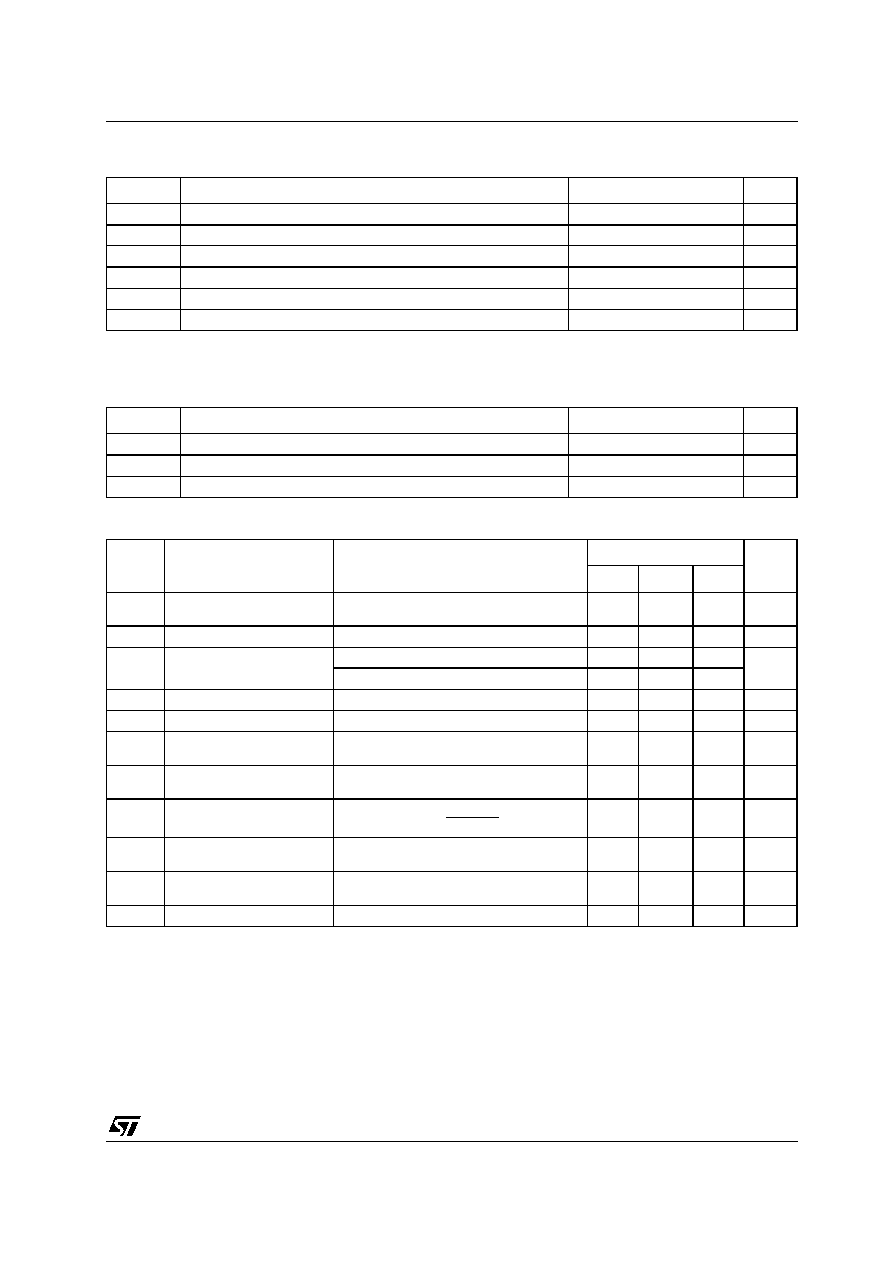
ABSOLUTE MAXIMUM RATINGS (Note 1, 2)
Note 1: Absolute Maximum Ratings are those values beyond which the safety of the device cannot be guaranteed. They are not meant to
imply that the device should be operated at these limits. The table of electrical characteristics provide conditions for actual device operation.
Note 2: Unless otherwise specified, all voltage are referenced to ground.
RECOMMENDED OPERATING CONDITIONS
ELECTRICAL CHARACTERISTICS (V
CC
= 5V
±
10%, unless otherwise specified, See Note 1)
Note 1: Unless otherwise specified, min/max limits apply across the recommended operating temperature range.
All typical are given for V
CC
= 5V and T
a
= 25∞C
Symbol
Parameter
Value
Unit
V
CC
Supply Voltage
7
V
V
CM
Input Common Mode Range
±
14
V
V
DIFF
Differential Input Voltage
±
14
V
V
IN
Enable Input Voltage
7
V
I
OMAX
Maximum Current per Output
±
25
mA
T
stg
Storage Temperature Range
-65 to +150
∞C
Symbol
Parameter
Value
Unit
V
CC
Supply Voltage
4.5 to 5.5
V
T
A
Operating Temperature Range
-40 to +85
∞C
t
r
, t
f
Maximum Enable Input Rise or Fall Times
500
ns
Symbol
Parameter
Test Conditions
Value
Unit
Min.
Typ.
Max.
V
TH
Minimum Differential Input
Voltage
V
OUT
= V
OH
or V
OL
,
-7V < V
CM
< 7V
-200
35
200
mV
R
IN
Input Resistance
V
IN
= -7V, 7V
Other Input = GND
5
6.8
10
K
I
IN
Input Current
V
IN
= 10V
Other Input = GND
1.1
1.5
mA
V
IN
= -10V
Other Input = GND
-2
-2.5
V
OH
High Level Output Voltage
V
DIFF
= 1V
I
OUT
= -6mA
3.8
4.2
V
V
OL
Low Level Output Voltage
V
DIFF
= -1V
I
OUT
= 6mA
0.2
0.3
V
V
IH
Minimum Enable High Input
Level Voltage
2
V
V
IL
Minimum Enable Low Input
Level Voltage
0.8
V
I
OZ
3-STATE Output Leakage
Current
V
OUT
= V
CC
or GND
ENABLE = V
IL
ENABLE = V
IH
±0.5
±5
µ
A
I
I
Maximum Enable Input
Current
V
IN
= V
CC
or GND
±1
µ
A
I
CC
Quiescent Power Supply
Current
V
CC
= Max, V
(DIFF)
= 1V
16
23
mA
V
HYST
Input Hysteresis
V
CM
= 0V
60
mV

ST26C32A
4/10
SWITCHING CHARACTERISTICS (V
CC
= 5V
±
10%, See Note 1)
Note 1: Unless otherwise specified, min/max limits apply across the recommended operating temperature range.
All typical are given for V
CC
=5V and T
a
= 25∞C.
Symbol
Parameter
Test Conditions
Value
Unit
Min.
Typ.
Max.
t
PLH
t
PHL
Propagation Delay Input to
Output
C
L
= 50pF
V
DIFF
= 2.5V
V
CM
= 0V
19
30
ns
t
RISE
t
FALL
Output Rise and Fall Times C
L
= 50pF
V
DIFF
= 2.5V
V
CM
= 0V
4
9
ns
t
PZH
t
PZL
Propagation Enable Time to
Output
C
L
= 50pF
V
DIFF
= 2.5V
R
L
= 1000
13
23
ns
t
PHZ
t
PLZ
Propagation Disable Time
to Output
C
L
= 50pF
V
DIFF
= 2.5V
R
L
= 1000
13
22
ns
D
R
Data Rate
C
L
= 50pF
V
DIFF
= 2.5V
All Outputs Loaded and Switching
10
20
Mbits/s

