 | –≠–ª–µ–∫—Ç—Ä–æ–Ω–Ω—ã–π –∫–æ–º–ø–æ–Ω–µ–Ω—Ç: ST763ACN | –°–∫–∞—á–∞—Ç—å:  PDF PDF  ZIP ZIP |

1/10
November 2000
s
OUTPUT VOLTAGE 3.3V
s
SUPPLY VOLTAGE RANGE FROM 3.3V TO
11V
s
GUARANTEED OUTPUT CURRENT: 500mA
s
TYPICAL OPERATION FREQUENCY:
200KHz
s
VERY LOW QUIESCENT CURRENT: 0.6mA
ON MODE 0.2
µ
A OFF MODE
s
SWITCH ON/OFF CONTROL
s
TYPICAL EFFICENCY: 90%
s
OPERATING TEMPERATURE RANGE:
-40∞C TO 85∞C
s
AVAILABLE IN SO-8 AND DIP-8 PACKAGES
DESCRIPTION
The ST763A is a step-down switching regulator . It
operates from 3.3V to 11V giving a fixed 3.3V
output voltage, delivering up to 500mA. The
mainly features are typical efficiency of 90%,
quiescent current of 0.6mA, and only 0.2
µ
A in
shut-down.
The PWM current mode control provides precise
output regulation and very good transient
response. Output voltage accuracy is guaranteed
to be
±
5% over line, load and temperature
variations. A minimum number of external
components is used and the fixed frequency
switching allows easy filtering of output ripple and
noise.
Other features of this ddevice are cycle-by-clicle
current limiting, overcurrent limiting, under voltage
lockout and programmable soft-start protection.
A 22
µ
H inductor works in most applications, so no
sophisticated design is necessary.
Package available are SO-8 and DIP-8.
Typical application are in 5V to 3.3V converters,
cellular phones, portable instruments, hand-held
computers, and peripherals.
ST763A
SERIES
3.3V STEP DOWN
CURRENT MODE PWM DC-DC CONVERTERS
SCHEMATIC DIAGRAM
DIP-8
SO-8

ST763A SERIES
2/10
ABSOLUTE MAXIMUM RATINGS
Absolute Maximum Ratings are those values beyond which damage to the device may occur. Functional operation under these condition is
not implied.
THERMAL DATA
(*) This value depends from thermal design of PCB on which the device is mounted.
ORDERING CODES
Symbol
Parameter≤
Value
Unit
V
CC
DC Input Voltage
-0.3 to 12
V
V
LX
Switch Pin Voltage
-0.3 to (V
CC
+ 0.3)
V
V
SHDN
Shutdown Voltage (SHDN)
-0.3 to (V
CC
+ 0.3)
V
V
S
,V
C
Soft Start (SS) and Compensation Capacitor (CC) Pins Voltage
-0.3 to (V
CC
+ 0.3)
V
I
LX
Switching Peak Current
2
A
I
REF
Reference Current
2.5
mA
P
TOT
Continuous Power Dissipation at T
A
=70∞C (DIP-8)
(SO-8)
550
344
mW
mW
T
stg
Storage Temperature Range
-40 to +150
∞C
T
op
Operating Junction Temperature Range (AC series)
(AB series)
0 to +70
-40 to +85
∞C
∞C
Symbol
Parameter
SO-8
DIP-8
Unit
R
thj-amb
Thermal Resistance Junction-ambient (*)
160
100
∞C/W
TYPE
DIP8
SO-8
SO-8 (T&R)
ST763AB
ST763ABN
ST763ABD
ST763ABDTR
ST763AC
ST763ACN
ST763ACD
ST763ACDTR

ST763A SERIES
3/10
CONNECTION DIAGRAM (top view)
PIN DESCRIPTION
Pin N∞
Symbol
Name and Function
1
SHDN
Shutdown control (active low): If connected to GND the IC is in shutdown.
Connect to V
CC
for normal operation (ON MODE)
2
REF
Reference Output Voltage:(1.25V): Bypass to GND with 47nF capacitor
3
SS
Soft Start: a capacitor between SS and GND provides soft-start and short-circuit
protections.
4
CC
Compensation Capacitor Input: externally compensates the outer (voltage)
feedback loop. Connect to OUT with 330pF capacitor
5
OUT
Output Voltage Sense Input: provides regulation of feedback sensing. Connect to
3.3V output.
6
GND
Ground
7
LX
Switch Output. Drain of internal P-Channel Power MOSFET
8
V
CC
Supply Voltage Input. Bypass to GND with 1
µ
F ceramic capacitance and large
value electrolytic capacitor in parallel. The 1
µ
F capacitor must be as close as
possible to the GND and V
CC
pins

ST763A SERIES
4/10
ELECTRICAL CHARACTERISTICS (V
CC
=5V, I
O
= 0mA, T
A
= T
MIN
to T
MAX
, unless otherwise specified.)
TYPICAL APPLICATION CIRCUIT
Symbol
Parameter
Test Conditions
Min.
Typ.
Max.
Unit
V
CC
Input Voltage
3.3
11
V
V
O
Output Voltage
V
CC
= 4 to 11V
I
O
=0 to 300mA
V
CC
= 4.75 to 11V I
O
=0 to 500mA
3.135
3.135
3.3
3.3
3.465
3.465
V
V
V
O
Line Regulation
0.13
%/V
V
O
Load Regulatio
I
O
= 1 to 500mA
0.005
%/mA
Power Efficency
I
O
=300mA
I
O
=100mA
88
90
%
%
I
SUPPLY
Supply Current
ON Mode (Including Switch Current)
OFF Mode
0.6
0.2
2.5
100
mA
µ
A
V
IH
SHDN Input High Threshold
2
V
V
IL
SHDN Input Low Threshold
0.25
V
I
SHDN
Shutdown Input Leakage
Current
1
µ
A
V
LOCK
Under Voltage Lockout
V
CC
Falling
2.7
3
V
R
DS(on)
LX On Resistance
I
LX
=500mA
1
I
LEAK
LX Leakage Current
V
CC
= 12V
V
LX
= 0V
10
nA
V
REF
Reference Voltage
T
A
= 25∞C
1.18
1.25
1.32
V
V
REF
Temeperature Reference
Drift
T
A
= T
MIN
to T
MAX
50
ppm/∞C
f
OSC
Switching Frequency
159
200
212.5
KHz
R
C
Compensation Pin
Impedance
7500
CC
SS
REF
SHDN
Vcc
Lx
OUT
GND
+
470 pF
220 µF
1 µF
1500 pF
100 µF
22 µH
Vout
Vin
0.047 µF
STPS330U
+
ST763A SERIES
5/10
TYPICAL PERFORMANCE CHARACTERISTICS (unless otherwise specified T
j
= 25∞C
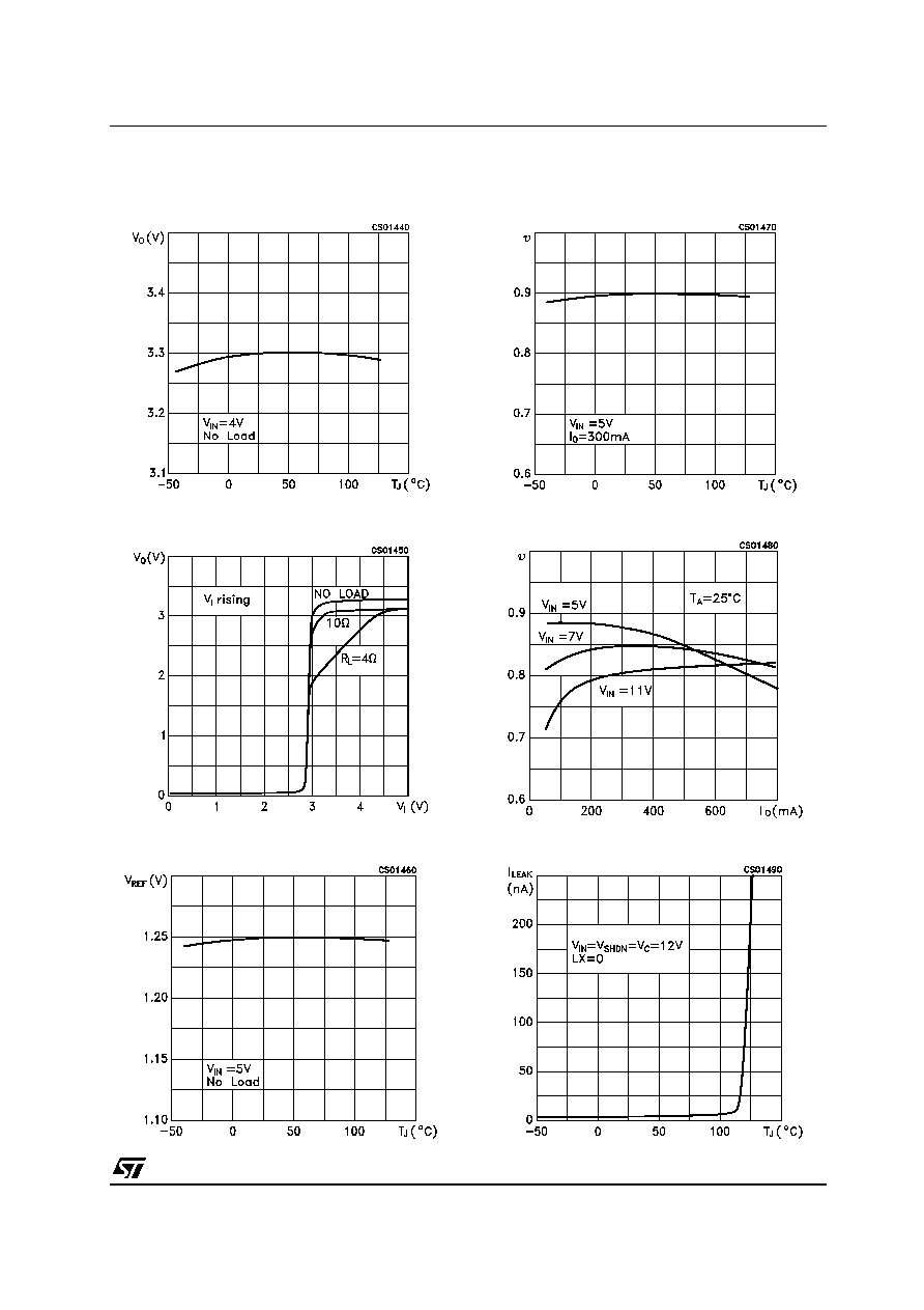
Figure 1 : Output Voltage vs Temperature
Figure 2 : Output Voltage vs Input Voltage
Figure 3 : Reference Voltage vs Temperature
Figure 4 : Efficency vs Temperature
Figure 5 : Efficency vs Output Current
Figure 6 : LX Leakage Current vs Temperature