 | –≠–ª–µ–∫—Ç—Ä–æ–Ω–Ω—ã–π –∫–æ–º–ø–æ–Ω–µ–Ω—Ç: START499 | –°–∫–∞—á–∞—Ç—å:  PDF PDF  ZIP ZIP |

1/7
July, 3 2002
START499
NPN Silicon RF Transistor
SOT343 (SC70)
ORDER CODE
START499TR
BRANDING
499
APPLICATIONS
∑ PA FOR DECT OR PHS
∑ PA STAGE FOR WIRELESS LAN AND
BLUETOOTH @ 2.5GHz
∑ UHF-VHF PRE POWER AMPLIFIER
∑ HIGH EFFICIENCY
∑ HIGH GAIN
∑ LINEAR AND NON LINEAR OPERATION
∑ TRANSITION FREQUENCY 42GHz
∑ ULTRA MINIATURE SOT343 (SC70) PACKAGE
DESCRIPTION
START499 is a product of the START family that
provide the market with a Si state-of-art RF process.
Manufactured in St 3rd generation bipolar process, it
offers the highest power, gain and efficiency in
SOT343 for given breakdown voltage (BVceo).
Suitable for a wide range of applications up to 5GHz,
it shows a performance level achieved before with
GaAs products only.
ABSOLUTE MAXIMUM RATINGS
Symbol
Parameter
Value
Unit
V
ceo
Collector emitter voltage
4.5
V
V
cbo
Collector base voltage
15
V
V
ebo
Emitter base voltage
1.5
V
I
c
Collector current
600
mA
I
b
Base current
32
mA
P
tot
Total dissipation at T
S
= 60
o
C
600
mW
T
stg
Storage temperature
-65 to 150
o
C
T
j
Max. operating junction temperature
150
o
C
R
thjs
Thermal Resistance Junction soldering point
150
o
C/W
ABSOLUTE MAXIMUM RATINGS

START499
2/7
Symbol
Parameter
Test Conditions
Min.
Typ.
Max.
Unit
I
cbo
Collector cutoff current
Vcb = 5V, Ie = 0A
1.2
µ
A
I
ebo
Emitter-base cutoff
current
Veb = 1.5V, Ic = 0A
120
µ
A
Hfe
DC current gain
Ic = 160mA, Vce = 4V
160
G
Power gain
Ic =200mA, Vce = 3V, f = 1.8GHz
15
dB
P
-1dB
1dB compression point
Ic = 200mA,Vce = 3V, f = 1.8GHz
23.5
dBm
IP3
Ouput third order
intercept point
Ic = 200mA,Vce = 3V, f = 1.8GHz
33.5
dBm
NF
Noise Figure
Ic = 200mA,Vce = 3V, f = 1.8GHz
3.3
dB
ELECTRICAL CHARACTERISTICS (T
j
=25
o
C,unless otherwise specified)
QUICK REFERENCE DATA
MODE OF OPERATION
f
(GHz)
V
CE
(V)
P
L
(dBm)
G
P
(dB)
(%)
Class-AB (Icq = 5mA)
1.9
3.6
26
12
typ. 68
PINOUT
PIN CONNECTION
Pin No.
Description
1
BASE
3
COLLECTOR
2,4
EMITTER
SOT343
4
1
2
3
Top view
3/7
START499
C
Transistor
Chip
B'
C'
E'
L=0.1 nH
L=0.5 nH
L3
L5
L6
C2
C=30 fF
.
.
L=0.1 nH
L1
L=0.15 nH
L=0.05 nH
L2
C=780 fF
C=640 fF
C1
C3
E
.
.
L=0.5 nH
L4
B
.
.
C
Transistor
Chip
B'
C'
E'
L=0.1 nH
L=0.5 nH
L3
L5
L6
C2
C=30 fF
.
.
L=0.1 nH
L1
L=0.15 nH
L=0.05 nH
L2
C=780 fF
C=640 fF
C1
C3
E
.
.
L=0.5 nH
L4
B
.
.
Symbol
Value
Symbol
Value
Symbol
Value
TMEAS
27.0
FC
0.81
XJBC
0.51
IS
3.27E-16
EG
1.12
XTI
3.68
ISE
13.08E-12
NF
1
BF
332
NR
1
NE
3.2
VAF
70
ISC
7.89E-15
BR
9.75
VAR
2.1
IKF
{3.948*((T(
o
C)+273.15)/
300.15)^(-1.7)}
NC
1.5
TF
3.4E-12
TR
7E-10
PTF
38
VTF
29.7
XTF
16.3
ITF
5.01
MJE
0.341
RB
2.58
RBM
0.83
MJC
0.312
RC
0.597
RE
0.066
MJS
0.297
CJE
3048E-15
VJE
1.09
IKR
57.3E-3
CJC
930E-15
VJC
0.695
XTB
-0.82
CJS
510E-15
VJS
0.507
SPICE PARAMETERS (Gummel-Poon Model, Berkley-SPICE 2G.6 Syntax)
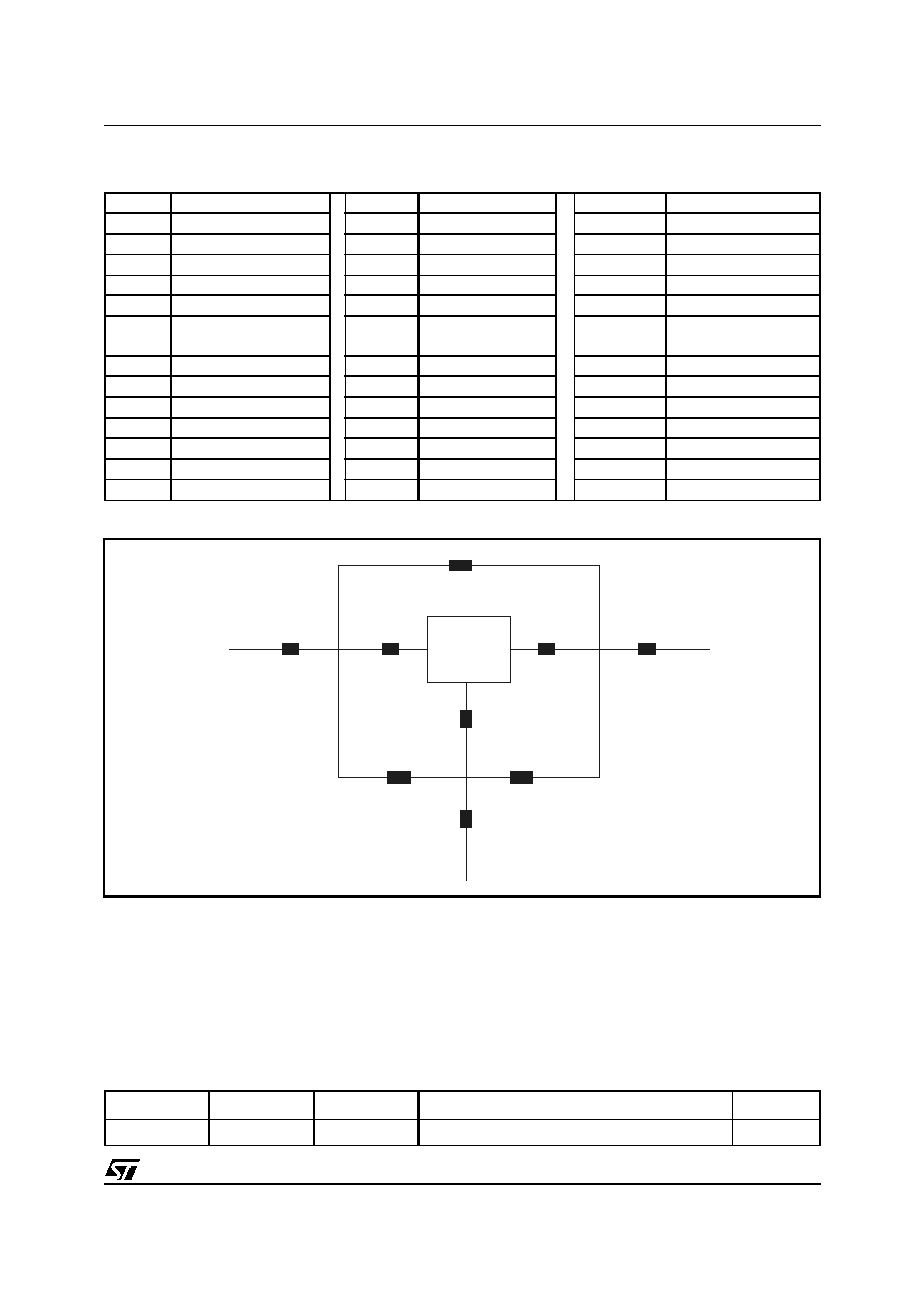
PACKAGE EQUIVALENT CIRCUIT
TRANSISTOR CHIP DATA
FOR MORE ACCURACY SIMULATION IN SATURATION REGION :
Adding the 5 Spice parameters showed in Table A and using ST Spice Library (available on request) you
can achieve a more accuracy simulation in the saturation region. ST Spice library is compatible with
following simulators: ELDO MENTOR (any version), SPECTRE CADENCE (any version), ADS (version
2001 only).
Table A (Spice Parameters extracted in saturation region)
RW
Vjj
ENP
VRP
RP
1.034
0.755
2.235
{7.2*((TEMPER+273.15)/300.15)^(0.125)}
0.33E-6
In order to avoid high complexity of the package equivalent circuit, the two emitter leads of SOT-343
package are combined in one electrical connection.

START499
4/7
FREQ
IS
11
I
IS
21
I
IS
12
I
S
12
IS
22
I
S
22
(MHz)
0.1
0.669
-158
65.164
124
0.008
47
0.635
-107
0.5
0.778
-179
15.773
105
0.013
81
0.589
-164
0.9
0.781
174
8.622
107
0.021
119
0.600
-174
1
0.780
173
7.535
109
0.021
134
0.598
-176
1.5
0.782
167
5.203
120
0.061
160
0.600
180
1.8
0.764
162
4.229
122
0.062
171
0.605
177
2
0.765
159
3.896
125
0.090
173
0.600
176
2.5
0.725
153
3.150
131
0.132
179
0.590
174
3
0.687
148
2.364
138
0.152
170
0.575
171
3.5
0.662
142
1.806
152
0.211
161
0.569
167
4
0.677
139
1.558
165
0.263
154
0.586
162
S
11
S
21
COMMON EMITTER S-PARAMETERS ( V
CE
= 2V, I
C
= 200mA )
5/7
START499
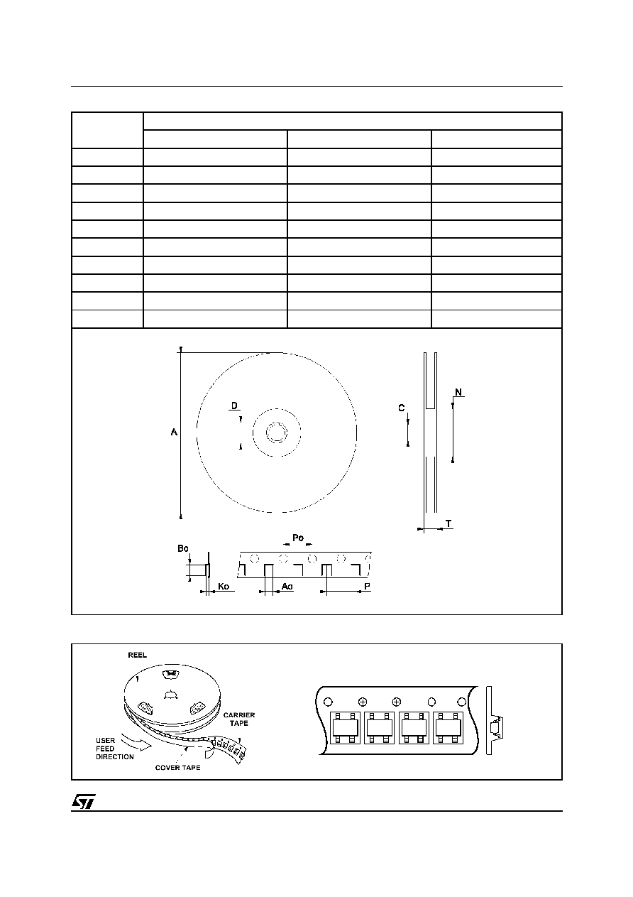
TAPE & REEL DIMENSIONS
mm
MIN.
TYP.
MAX
A
178.5
179
179.5
C
12.8
13.0
13.5
D
20.2
N
54.5
55
55.5
T
14.4
Ao
2.25
Bo
2.7
Ko
1.2
Po
3.8 (cumulative 10 Po)
4.0
4.2 (cumulative 10 Po)
P
4.0
DEVICE ORIENTATION
TOP
VIEW END
VIEW
499
499
499
499