 | –≠–ª–µ–∫—Ç—Ä–æ–Ω–Ω—ã–π –∫–æ–º–ø–æ–Ω–µ–Ω—Ç: STB19NB20 | –°–∫–∞—á–∞—Ç—å:  PDF PDF  ZIP ZIP |

STB19NB20
N - CHANNEL ENHANCEMENT MODE
PowerMESH
TM
MOSFET
s
TYPICAL R
DS(on)
= 0.150
s
EXTREMELY HIGH dv/dt CAPABILITY
s
100% AVALANCHE TESTED
s
VERY LOW INTRINSIC CAPACITANCES
s
GATE CHARGE MINIMIZED
s
FOR THROUGH-HOLE VERSION CONTACT
SALES OFFICE
DESCRIPTION
Using the latest high voltage MESH OVERLAY
TM
process, STMicroelectronics has designed an
advanced family of
Power MOSFETs
with
outstanding
performance.
The
new
patent
pending strip layout coupled with the Company's
proprietary edge termination structure, gives the
lowest RDS(on) per area, exceptional avalanche
and dv/dt capabilities and unrivalled gate charge
and switching characteristics.
APPLICATIONS
s
HIGH CURRENT, HIGH SPEED SWITCHING
s
SWITCH MODE POWER SUPPLIES (SMPS)
s
DC-AC CONVERTERS FOR WELDING
EQUIPMENT AND UNINTERRUPTIBLE
POWER SUPPLIES AND MOTOR DRIVE
Æ
June 1998
INTERNAL SCHEMATIC DIAGRAM
ABSOLUTE MAXIMUM RATINGS
Symb ol
Parameter
Value
Unit
V
DS
Drain-source Voltage (V
GS
= 0)
200
V
V
DGR
Drain- gate Voltage (R
GS
= 20 k
)
200
V
V
GS
G ate-source Volt age
±
30
V
I
D
Drain Current (continuous) at T
c
= 25
o
C
19
A
I
D
Drain Current (continuous) at T
c
= 100
o
C
12
A
I
DM
(
∑
)
Drain Current (pulsed)
76
A
P
tot
T otal Dissipation at T
c
= 25
o
C
125
W
Derating Factor
1
W /
o
C
dv/dt(
1
)
Peak Diode Recovery voltage slope
5.5
V/ns
T
s tg
Storage T emperature
-65 to 150
o
C
T
j
Max. O perat ing Junct ion T emperature
150
o
C
(
∑
) Pulse width limited by safe operating area
(
1
) I
SD
19A, di/dt
300 A/
µ
s, V
DD
V
(BR)DSS
, Tj
T
JMAX
1
3
D
2
PAK
TO-263
(suffix "T4")
TYPE
V
DSS
R
DS(on)
I
D
ST B19NB20
200 V
< 0.180
19 A
1/8

THERMAL DATA
R
thj -case
Thermal Resistance Junction-case
Max
1
o
C/W
R
thj -amb
R
thc-sink
T
l
Thermal Resistance Junction-ambient
Max
Thermal Resistance Case-sink
Typ
Maximum Lead Temperature F or Soldering Purpose
62.5
0.5
300
o
C/W
o
C/W
o
C
AVALANCHE CHARACTERISTICS
Symbo l
Parameter
Max Value
Unit
I
AR
Avalanche Current, Repetitive or Not-Repetitive
(pulse width limited by T
j
max)
19
A
E
AS
Single Pulse Avalanche Energy
(starting T
j
= 25
o
C, I
D
= I
AR
, V
DD
= 50 V)
580
mJ
ELECTRICAL CHARACTERISTICS (T
case
= 25
o
C unless otherwise specified)
OFF
Symbo l
Parameter
Test Con ditions
Min.
Typ.
Max.
Unit
V
(BR)DSS
Drain-source
Breakdown Voltage
I
D
= 250
µ
A
V
GS
= 0
200
V
I
DSS
Zero Gat e Voltage
Drain Current (V
GS
= 0)
V
DS
= Max Rat ing
V
DS
= Max Rat ing
T
c
= 125
o
C
1
10
µ
A
µ
A
I
G SS
Gat e-body Leakage
Current (V
DS
= 0)
V
GS
=
±
30 V
±
100
nA
ON (
)
Symbo l
Parameter
Test Con ditions
Min.
Typ.
Max.
Unit
V
G S(th)
Gat e Threshold Voltage V
DS
= V
GS
I
D
= 250
µ
A
3
4
5
V
R
DS(on)
Static Drain-source On
Resistance
V
GS
= 10V
I
D
= 9. 5 A
0.150
0.180
I
D(o n)
On State Drain Current
V
DS
> I
D(o n)
x R
DS(on )ma x
V
GS
= 10 V
19
A
DYNAMIC
Symbo l
Parameter
Test Con ditions
Min.
Typ.
Max.
Unit
g
f s
(
)
Forward
Transconductance
V
DS
> I
D(o n)
x R
DS(on )ma x
I
D
=9.5 A
3
S
C
iss
C
os s
C
rss
Input Capacitance
Out put Capacitance
Reverse Transfer
Capacitance
V
DS
= 25 V
f = 1 MHz
V
GS
= 0
1000
285
45
1350
385
60
pF
pF
pF
STB19NB20
2/8

ELECTRICAL CHARACTERISTICS (continued)
SWITCHING ON
Symbo l
Parameter
Test Con ditions
Min.
Typ.
Max.
Unit
t
d(on)
t
r
Turn-on Time
Rise Time
V
DD
= 100 V
I
D
= 9.5 A
R
G
= 4.7
V
GS
= 10 V
(see t est circuit, f igure 3)
15
15
20
20
ns
ns
Q
g
Q
gs
Q
gd
Tot al G ate Charge
Gat e-Source Charge
Gat e-Drain Charge
V
DD
= 160 V
I
D
= 19 A V
GS
= 10 V
29
9.5
13
40
nC
nC
nC
SWITCHING OFF
Symbo l
Parameter
Test Con ditions
Min.
Typ.
Max.
Unit
t
r (Voff)
t
f
t
c
Off -volt age Rise T ime
Fall T ime
Cross-over Time
V
DD
= 160 V
I
D
= 19 A
R
G
= 4.7
V
G S
= 10 V
(see t est circuit, f igure 5)
10
10
20
15
15
30
ns
ns
ns
SOURCE DRAIN DIODE
Symbo l
Parameter
Test Con ditions
Min.
Typ.
Max.
Unit
I
SD
I
SDM
(
∑
)
Source-drain Current
Source-drain Current
(pulsed)
19
76
A
A
V
SD
(
)
Forward On Voltage
I
SD
=19 A
V
GS
= 0
1. 5
V
t
rr
Q
rr
I
RRM
Reverse Recovery
Time
Reverse Recovery
Charge
Reverse Recovery
Current
I
SD
=19 A
di/ dt = 100 A/
µ
s
V
DD
= 50 V
T
j
= 150
o
C
(see t est circuit, f igure 5)
210
1.5
14.5
ns
µ
C
A
(
) Pulsed: Pulse duration = 300
µ
s, duty cycle 1.5 %
(
∑
) Pulse width limited by safe operating area
Safe Operating Area
Thermal Impedance
STB19NB20
3/8
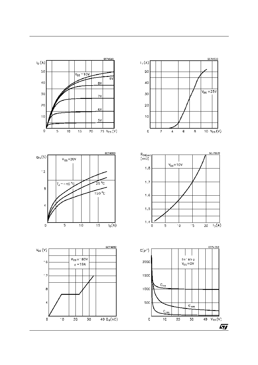
Output Characteristics
Transconductance
Gate Charge vs Gate-source Voltage
Transfer Characteristics
Static Drain-source On Resistance
Capacitance Variations
STB19NB20
4/8

Normalized Gate Threshold Voltage vs
Temperature
Source-drain Diode Forward Characteristics
Normalized On Resistance vs Temperature
STB19NB20
5/8