 | ÐлекÑÑоннÑй компоненÑ: STB4NC80Z | СкаÑаÑÑ:  PDF PDF  ZIP ZIP |
Äîêóìåíòàöèÿ è îïèñàíèÿ www.docs.chipfind.ru
1/13
December 2002
STP4NC80Z - STP4NC80ZFP
STB4NC80Z - STB4NC80Z-1
N-CHANNEL 800V - 2.4
- 4A TO-220/FP/D
2
PAK/I
2
PAK
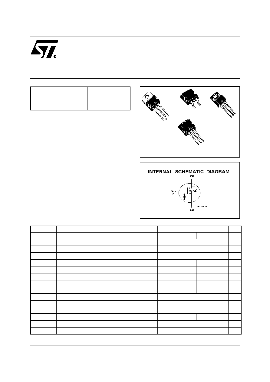
Zener-Protected PowerMESHTMIII MOSFET
(1)I
SD
4A, di/dt
100A/µs, V
DD
V
(BR)DSS
, T
j
T
JMAX
.
(*)Pulse width Limited by maximum temperature allowed
TO-220
1
2
3
TO-220FP
1
2
3
I
2
PAK
(Tabless TO-220)
1
3
D
2
PAK
s
TYPICAL R
DS
(on) = 2.4
s
EXTREMELY HIGH dv/dt AND CAPABILITY
GATE-TO- SOURCE ZENER DIODES
s
100% AVALANCHE TESTED
s
VERY LOW GATE INPUT RESISTANCE
s
GATE CHARGE MINIMIZED
DESCRIPTION
The third generation of MESH OVERLAYTM Power
MOSFETs for very high voltage exhibits unsurpassed
on-resistance per unit area while integrating back-to-
back Zener diodes between gate and source. Such ar-
rangement gives extra ESD capability with higher rug-
gedness performance as requested by a large variety
of single-switch applications.
APPLICATIONS
s
SINGLE-ENDED SMPS IN MONITORS,
COMPUTER AND INDUSTRIAL APPLICATION
s
WELDING EQUIPMENT
ABSOLUTE MAXIMUM RATINGS
(·)Pulse width limited by safe operating area
TYPE
V
DSS
R
DS(on)
I
D
STP4NC80Z/FP
800V
< 2.8
4 A
STB4NC80Z/-1
800V
< 2.8
4 A
Symbol
Parameter
Value
Unit
STP(B)4NC80Z(-1)
STP4NC80ZFP
V
DS
Drain-source Voltage (V
GS
= 0)
800
V
V
DGR
Drain-gate Voltage (R
GS
= 20 k
)
800
V
V
GS
Gate- source Voltage
± 25
V
I
D
Drain Current (continuos) at T
C
= 25°C
4
4(*)
A
I
D
Drain Current (continuos) at T
C
= 100°C
2.5
2.5(*)
A
I
DM
(
q
)
Drain Current (pulsed)
16
16(*)
A
P
TOT
Total Dissipation at T
C
= 25°C
100
35
W
Derating Factor
0.8
0.28
W/°C
I
GS
Gate-source Current
±50
mA
V
ESD(G-S)
Gate source ESD(HBM-C=100pF, R=15K
)
2.5
KV
dv/dt(1)
Peak Diode Recovery voltage slope
3
V/ns
V
ISO
Insulation Winthstand Voltage (DC)
--
2000
V
T
stg
Storage Temperature
65 to 150
°C
T
j
Max. Operating Junction Temperature
150
°C
STP4NC80Z - STP4NC80ZFP - STB4NC80Z - STB4NC80Z-1
2/13
THERMAL DATA
AVALANCHE CHARACTERISTICS
ELECTRICAL CHARACTERISTICS (TCASE = 25 °C UNLESS OTHERWISE SPECIFIED)
OFF
ON (1)
DYNAMIC
TO-220 / D
2
PAK /
I
2
PAK
TO-220FP
Rthj-case
Thermal Resistance Junction-case Max
1.25
3.57
°C/W
Rthj-amb
Thermal Resistance Junction-ambient Max
30
°C/W
T
l
Maximum Lead Temperature For Soldering Purpose
300
°C
Symbol
Parameter
Max Value
Unit
I
AR
Avalanche Current, Repetitive or Not-Repetitive
(pulse width limited by T
j
max)
4
A
E
AS
Single Pulse Avalanche Energy
(starting T
j
= 25 °C, I
D
= I
AR
, V
DD
= 50 V)
225
mJ
Symbol
Parameter
Test Conditions
Min.
Typ.
Max.
Unit
V
(BR)DSS
Drain-source
Breakdown Voltage
I
D
= 250 µA, V
GS
= 0
800
V
BV
DSS
/
T
J
Breakdown Voltage Temp.
Coefficient
I
D
= 1 mA, V
GS
= 0
0.9
V/°C
I
DSS
Zero Gate Voltage
Drain Current (V
GS
= 0)
V
DS
= Max Rating
1
µA
V
DS
= Max Rating, T
C
= 125 °C
50
µA
I
GSS
Gate-body Leakage
Current (V
DS
= 0)
V
GS
= ±20V
±10
µA
Symbol
Parameter
Test Conditions
Min.
Typ.
Max.
Unit
V
GS(th)
Gate Threshold Voltage
V
DS
= V
GS
, I
D
= 250µA
3
4
5
V
R
DS(on)
Static Drain-source On
Resistance
V
GS
= 10V, I
D
= 2 A
2.4
2.8
Symbol
Parameter
Test Conditions
Min.
Typ.
Max.
Unit
g
fs
(1)
Forward Transconductance
V
DS
> I
D(on)
x R
DS(on)max,
I
D
= 2A
4
S
C
iss
Input Capacitance
V
DS
= 25V, f = 1 MHz, V
GS
= 0
1200
pF
C
oss
Output Capacitance
90
pF
C
rss
Reverse Transfer
Capacitance
11
pF

3/13
STP4NC80Z - STP4NC80ZFP - STB4NC80Z - STB4NC80Z-1
ELECTRICAL CHARACTERISTICS (CONTINUED)
SWITCHING ON
SWITCHING OFF
SOURCE DRAIN DIODE
GATE-SOURCE ZENER DIODE
Note: 1. Pulsed: Pulse duration = 300 µs, duty cycle 1.5 %.
2. Pulse width limited by safe operating area.
3.
V
BV
=
T (25°-T) BV
GSO
(25°)
PROTECTION FEATURES OF GATE-TO-SOURCE ZENER DIODES
The built-in back-to-back Zener diodes have specifically been designed to enhance not only the device's
ESD capability, but also to make them safely absorb possible voltage transients that may occasionally
be applied from gate to source. In this respect the Zener voltage is appropriate to achieve an efficient
and cost-effective intervention to protect the device's integrity. These integrated Zener diodes thus avoid
the usage of external components.
Symbol
Parameter
Test Conditions
Min.
Typ.
Max.
Unit
t
d(on)
Turn-on Delay Time
V
DD
= 400 V, I
D
= 2 A
R
G
= 4.7
V
GS
= 10V
(see test circuit, Figure 3)
27
ns
t
r
Rise Time
10
ns
Q
g
Total Gate Charge
V
DD
= 640V, I
D
= 4A,
V
GS
= 10V
27
36.5
nC
Q
gs
Gate-Source Charge
7
nC
Q
gd
Gate-Drain Charge
10
nC
Symbol
Parameter
Test Conditions
Min.
Typ.
Max.
Unit
t
r(Voff)
Off-voltage Rise Time
V
DD
= 640V, I
D
= 4 A,
R
G
= 4.7
,
V
GS
= 10V
(see test circuit, Figure 5)
11
ns
t
f
Fall Time
10
ns
t
c
Cross-over Time
24
ns
Symbol
Parameter
Test Conditions
Min.
Typ.
Max.
Unit
I
SD
Source-drain Current
4
A
I
SDM
(2)
Source-drain Current (pulsed)
16
A
V
SD
(1)
Forward On Voltage
I
SD
= 4 A, V
GS
= 0
1.6
V
t
rr
Reverse Recovery Time
I
SD
= 4 A, di/dt = 100A/µs,
V
DD
= 50V, T
j
= 150°C
(see test circuit, Figure 5)
560
ns
Q
rr
Reverse Recovery Charge
3.4
µC
I
RRM
Reverse Recovery Current
13
A
Symbol
Parameter
Test Conditions
Min.
Typ.
Max.
Unit
BV
GSO
Gate-Source Breakdown
Voltage
Igs=± 1mA (Open Drain)
25
V
T
Voltage Thermal Coefficient
T=25°C Note(3)
1.3
10
-4
/°C
Rz
Dynamic Resistance
I
D
= 50 mA,
90
STP4NC80Z - STP4NC80ZFP - STB4NC80Z - STB4NC80Z-1
4/13
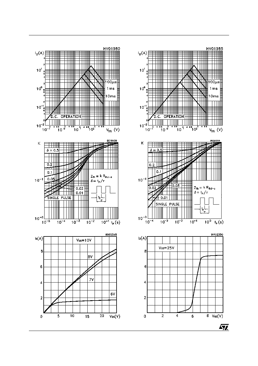
Safe Operating Area For TO-220FP
Safe Operating Area For TO-220/D²PAK/I²PAK
Output Characteristics
Thermal Impedance For TO-220/D²PAK/I²PAK
Thermal Impedance For TO-220FP
Transfer Characteristics
5/13
STP4NC80Z - STP4NC80ZFP - STB4NC80Z - STB4NC80Z-1
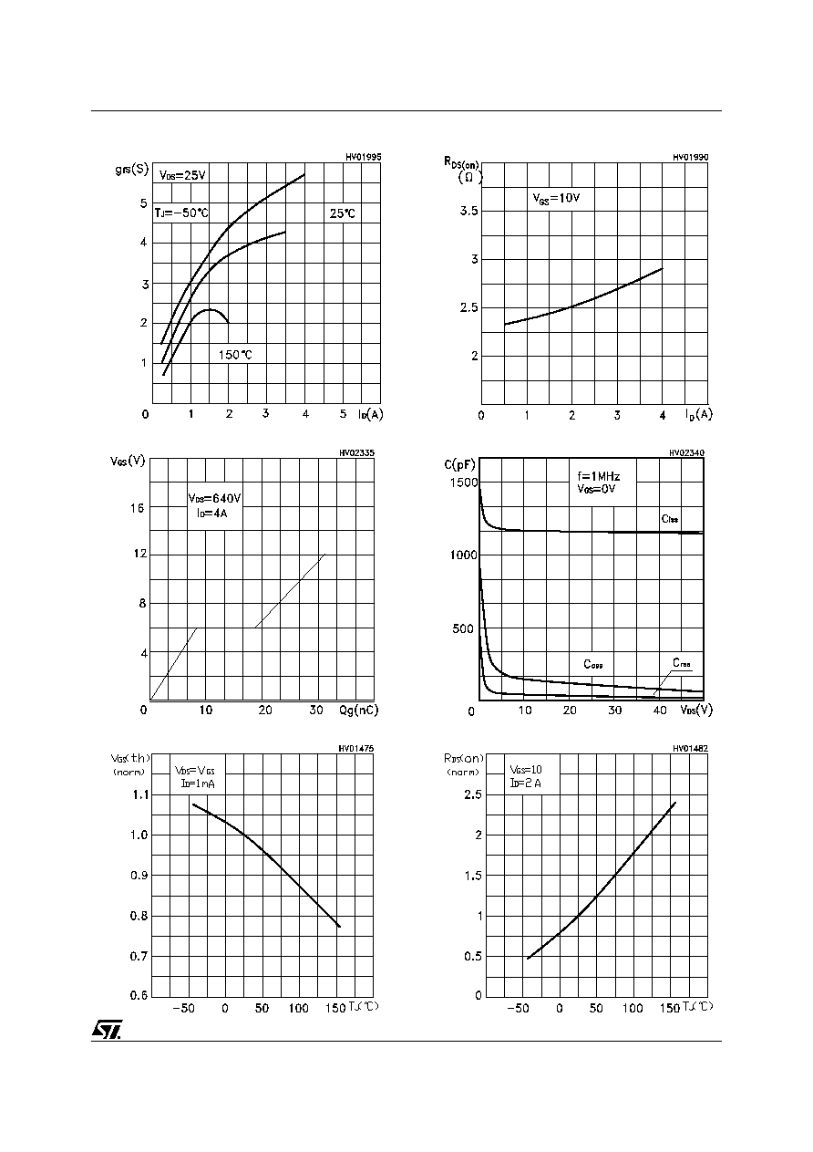
Normalized On Resistance vs Temperature
Normalized Gate Threshold Voltage vs Temp.
Capacitance Variations
Gate Charge vs Gate-source Voltage
Static Drain-source On Resistance
Transconductance