
1/11
February 2005
STP80NF10
STB80NF10
N-CHANNEL 100V - 0.012
- 80A - TO-220/D
2
PAK
LOW GATE CHARGE STripFETTMII MOSFET
Table 1: General Features
s
TYPICAL R
DS
(on) = 0.012
s
EXCEPTIONAL dv/dt CAPABILITY
s
100% AVALANCHE TESTED
s
APPLICATION ORIENTED
CHARACTERIZATION
DESCRIPTION
This MOSFET series realized with STMicroelec-
tronics unique STripFET process has specifically
been designed to minimize input capacitance and
gate charge. It is therefore suitable as primary
switch in advanced high-efficiency isolated DC-DC
converters for Telecom and Computer application.
It is also intended for any application with low gate
charge drive requirements.
APPLICATIONS
s
HIGH-EFFICIENCY DC-AC CONVERTERS
s
UPS AND MOTOR CONTROL
Table 2: Order Codes
Figure 1: Package
Figure 2: Internal Schematic Diagram
TYPE
V
DSS
R
DS(on)
I
D
STB80NF10
STP80NF10
100 V
100 V
< 0.015
< 0.015
80 A
80 A
TO-220
1
2
3
1
3
D
2
PAK
SALES TYPE
MARKING
PACKAGE
PACKAGING
STB80NF10T4
B80NF10@
D
2
PAK
TAPE & REEL
STP80NF10
P80NF10@
TO-220
TUBE
Rev. 3

STP80NF10 - STB80NF10
2/11
Table 3: Absolute Maximum ratings
(
q
) Pulse width limited by safe operating area
(*) Limited by Package
(1) I
SD
80A, di/dt
300A/µs, V
DD
V
(BR)DSS
, T
j
T
JMAX.
(2) Starting T
j
= 25∞C, I
D
= 80A, V
DD
= 50V
Table 4: Thermal Data
ELECTRICAL CHARACTERISTICS (T
CASE
=25∞C UNLESS OTHERWISE SPECIFIED)
Table 5: Off
Table 6: On
Symbol
Parameter
Value
Unit
V
DS
Drain-source Voltage (V
GS
= 0)
100
V
V
DGR
Drain-gate Voltage (R
GS
= 20 k
)
100
V
V
GS
Gate- source Voltage
±20
V
I
D
Drain Current (continuous) at T
C
= 25∞C
80
A
I
D
Drain Current (continuous) at T
C
= 100∞C
80 (*)
A
I
DM
( )
Drain Current (pulsed)
320
A
P
TOT
Total Dissipation at T
C
= 25∞C
300
W
Derating Factor
2
W/∞C
dv/dt (1)
Peak Diode Recovery voltage slope
7
V/ns
E
AS
(2)
Single Pulse Avalanche Energy
200
mJ
T
stg
Storage Temperature
≠55 to 175
∞C
T
j
Operating Junction Temperature
175
∞C
Rthj-case
Thermal Resistance Junction-case Max
0.5
∞C/W
Rthj-amb
Thermal Resistance Junction-ambient Max
62.5
∞C/W
T
l
Maximum Lead Temperature For Soldering Purpose
300
∞C
Symbol
Parameter
Test Conditions
Min.
Typ.
Max.
Unit
V
(BR)DSS
Drain-source
Breakdown Voltage
I
D
= 250 µA, V
GS
= 0
100
V
I
DSS
Zero Gate Voltage
Drain Current (V
GS
= 0)
V
DS
= Max Rating
1
µA
V
DS
= Max Rating, T
C
= 125∞C
10
µA
I
GSS
Gate-body Leakage
Current (V
DS
= 0)
V
GS
= ± 20V
±100
nA
Symbol
Parameter
Test Conditions
Min.
Typ.
Max.
Unit
V
GS(th)
Gate Threshold Voltage V
DS
= V
GS
, I
D
= 250µA
2
3
4
V
R
DS(on)
Static Drain-source On
Resistance
V
GS
= 10V, I
D
= 40 A
0.012
0.015
3/11
STP80NF10 - STB80NF10
ELECTRICAL CHARACTERISTICS (CONTINUED)
Table 7: Dynamic
Table 8: Switching On
Table 9: Switching Off
Table 10: Source Drain Diode
(1) Pulsed: Pulse duration = 300 µs, duty cycle 1.5 %.
(2) Pulse width limited by safe operating area.
Symbol
Parameter
Test Conditions
Min.
Typ.
Max.
Unit
g
fs
(1)
Forward Transconductance
V
DS
= 15V
,
I
D
= 40A
50
S
C
iss
C
oss
C
rss
Input Capacitance
Output Capacitance
Reverse Transfer
Capacitance
V
DS
= 25V, f = 1 MHz, V
GS
= 0
5500
700
175
pF
pF
pF
Symbol
Parameter
Test Conditions
Min.
Typ.
Max.
Unit
t
d(on)
t
r
Turn-on Delay Time
Rise Time
V
DD
= 50V, I
D
= 40A
R
G
= 4.7
V
GS
= 10V
(see Figure 14)
26
80
ns
ns
Q
g
Q
gs
Q
gd
Total Gate Charge
Gate-Source Charge
Gate-Drain Charge
V
DD
= 80V, I
D
= 80A,
V
GS
= 10V
135
23
51.3
182
nC
nC
nC
Symbol
Parameter
Test Conditions
Min.
Typ.
Max.
Unit
t
d(off)
t
f
Turn-off-Delay Time
Fall Time
V
DD
= 50V, I
D
= 40A,
R
G
=4.7
,
V
GS
= 10V
(see Figure 14)
116
60
ns
ns
Symbol
Parameter
Test Conditions
Min.
Typ.
Max.
Unit
I
SD
Source-drain Current
80
A
I
SDM
(2)
Source-drain Current (pulsed)
320
A
V
SD
(1)
Forward On Voltage
I
SD
= 80A, V
GS
= 0
1.3
V
t
rr
Q
rr
I
RRM
Reverse Recovery Time
Reverse Recovery Charge
Reverse Recovery Current
I
SD
= 80A, di/dt = 100A/µs,
V
DD
= 50V, T
j
= 150∞C
(see test circuit, Figure 5)
106
0.45
8.5
ns
µC
A
STP80NF10 - STB80NF10
4/11
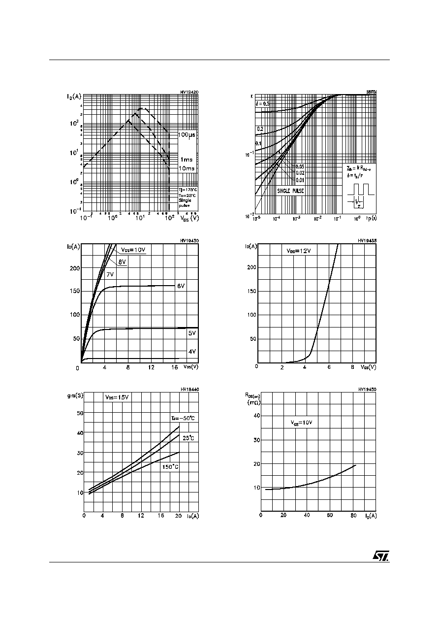
Figure 3: Safe Operating Area
Figure 4: Output Characteristics
Figure 5: Transconductance
Figure 6: Thermal Impedance
Figure 7: Transfer Characteristics
Figure 8: Static Drain-source On Resistance

5/11
STP80NF10 - STB80NF10
Figure 9: Gate Charge vs Gate-source Voltage
Figure 10: Normalized Gate Thereshold Volt-
age vs Temperature
Figure 11: Source-Drain Diode Forward Char-
acteristics
Figure 12: Capacitance Variations
Figure 13: Normalized On Resistance vs Tem-
perature

STP80NF10 - STB80NF10
6/11
Figure 14: Switching Times Test Circuit For
Resistive Load
Figure 15: Test Circuit For Inductive Load
Switching and Diode Recovery Times
Figure 16: Gate Charge Test Circuit

7/11
STP80NF10 - STB80NF10
DIM.
mm.
inch
MIN.
TYP
MAX.
MIN.
TYP.
MAX.
A
4.40
4.60
0.173
0.181
b
0.61
0.88
0.024
0.034
b1
1.15
1.70
0.045
0.066
c
0.49
0.70
0.019
0.027
D
15.25
15.75
0.60
0.620
E
10
10.40
0.393
0.409
e
2.40
2.70
0.094
0.106
e1
4.95
5.15
0.194
0.202
F
1.23
1.32
0.048
0.052
H1
6.20
6.60
0.244
0.256
J1
2.40
2.72
0.094
0.107
L
13
14
0.511
0.551
L1
3.50
3.93
0.137
0.154
L20
16.40
0.645
L30
28.90
1.137
¯P
3.75
3.85
0.147
0.151
Q
2.65
2.95
0.104
0.116
TO-220 MECHANICAL DATA

STP80NF10 - STB80NF10
8/11
TO-247 MECHANICAL DATA
1
DIM.
mm.
inch
MIN.
TYP
MAX.
MIN.
TYP.
MAX.
A
4.4
4.6
0.173
0.181
A1
2.49
2.69
0.098
0.106
A2
0.03
0.23
0.001
0.009
B
0.7
0.93
0.027
0.036
B2
1.14
1.7
0.044
0.067
C
0.45
0.6
0.017
0.023
C2
1.23
1.36
0.048
0.053
D
8.95
9.35
0.352
0.368
D1
8
0.315
E
10
10.4
0.393
E1
8.5
0.334
G
4.88
5.28
0.192
0.208
L
15
15.85
0.590
0.625
L2
1.27
1.4
0.050
0.055
L3
1.4
1.75
0.055
0.068
M
2.4
3.2
0.094
0.126
R
0.4
0.015
V2
0∫
4∫
D
2
PAK MECHANICAL DATA
3

9/11
STP80NF10 - STB80NF10
TAPE AND REEL SHIPMENT (suffix "T4")*
TUBE SHIPMENT (no suffix)*
D
2
PAK FOOTPRINT
* on sales type
DIM.
mm
inch
MIN.
MAX.
MIN.
MAX.
A
330
12.992
B
1.5
0.059
C
12.8
13.2
0.504
0.520
D
20.2
0795
G
24.4
26.4
0.960
1.039
N
100
3.937
T
30.4
1.197
BASE QTY
BULK QTY
1000
1000
REEL MECHANICAL DATA
DIM.
mm
inch
MIN.
MAX.
MIN.
MAX.
A0
10.5
10.7
0.413
0.421
B0
15.7
15.9
0.618
0.626
D
1.5
1.6
0.059
0.063
D1
1.59
1.61
0.062
0.063
E
1.65
1.85
0.065
0.073
F
11.4
11.6
0.449
0.456
K0
4.8
5.0
0.189
0.197
P0
3.9
4.1
0.153
0.161
P1
11.9
12.1
0.468
0.476
P2
1.9
2.1
0.075
0.082
R
50
1.574
T
0.25
0.35
0.0098 0.0137
W
23.7
24.3
0.933
0.956
TAPE MECHANICAL DATA

STP80NF10 - STB80NF10
10/11
Table 11: Revision History
Date
Revision
Description of Changes
04-Nov-2003
1
NEW DATASHEET ACCORDING TO PCN DSG-TRA/03/382
22-Nov-2004
2
NEW STYLESHEET, NO CONTENT CHANGE
21-Jan-2005
3
Value Change on Table 3

11/11
STP80NF10 - STB80NF10
Information furnished is believed to be accurate and reliable. However, STMicroelectronics assumes no responsibility for the consequences
of use of such information nor for any infringement of patents or other rights of third parties which may result from its use. No license is granted
by implication or otherwise under any patent or patent rights of STMicroelectronics. Specifications mentioned in this publication are subject
to change without notice. This publication supersedes and replaces all information previously supplied. STMicroelectronics products are not
authorized for use as critical components in life support devices or systems without express written approval of STMicroelectronics.
The ST logo is a registered trademark of STMicroelectronics
All other names are the property of their respective owners
© 2005 STMicroelectronics - All Rights Reserved
STMicroelectronics group of companies
Australia - Belgium - Brazil - Canada - China - Czech Republic - Finland - France - Germany - Hong Kong - India - Israel - Italy - Japan -
Malaysia - Malta - Morocco - Singapore - Spain - Sweden - Switzerland - United Kingdom - United States of America