 | –≠–ª–µ–∫—Ç—Ä–æ–Ω–Ω—ã–π –∫–æ–º–ø–æ–Ω–µ–Ω—Ç: STBV42 | –°–∫–∞—á–∞—Ç—å:  PDF PDF  ZIP ZIP |
STBV42
HIGH VOLTAGE FAST-SWITCHING
NPN POWER TRANSISTOR
s
MEDIUM VOLTAGE CAPABILITY
s
LOW SPREAD OF DYNAMIC PARAMETERS
s
MINIMUM LOT-TO-LOT SPREAD FOR
RELIABLE OPERATION
s
VERY HIGH SWITCHING SPEED
APPLICATIONS:
s
ELECTRONIC BALLASTS FOR
FLUORESCENT LIGHTING
DESCRIPTION
The device is manufactured using high voltage
Multi Epitaxial Planar technology for high
switching speeds and medium voltage capability.
It uses a Cellular Emitter structure with planar
edge termination to enhance switching speeds
while maintaining the wide RBSOA.
The STBV42 is designed for use in compact
fluorescent lamp application.
Æ
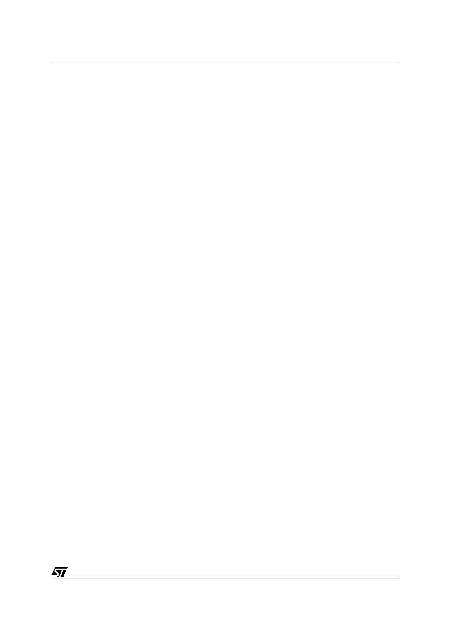
INTERNAL SCHEMATIC DIAGRAM
September 2001
ABSOLUTE MAXIMUM RATINGS
Symbol
Parameter
Value
Unit
V
CES
Collector-Emitter Voltage (V
BE
= 0)
700
V
V
CEO
Collector-Emitter Voltage (I
B
= 0)
400
V
V
EBO
Emitter-Base Voltage (I
C
= 0)
9
V
I
C
Collector Current
1
A
I
CM
Collector Peak Current (t
p
< 5 ms)
2
A
I
B
Base Current
0.5
A
I
BM
Base Peak Current (t
p
< 5 ms)
1
A
P
tot
Total Dissipation at T
amb
= 25
o
C
1
W
T
stg
Storage Temperature
-65 to 150
o
C
T
j
Max. Operating Junction Temperature
150
o
C
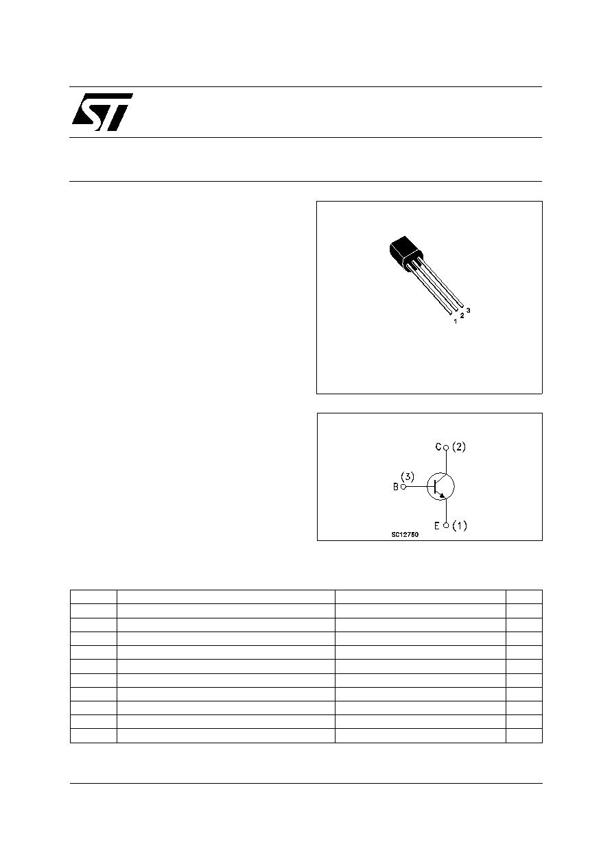
TO-92
1/5

THERMAL DATA
R
thj-amb
Thermal Resistance Junction-ambient Max
120
o
C/W
ELECTRICAL CHARACTERISTICS (T
case
= 25
o
C unless otherwise specified)
Symbol
Parameter
Test Conditions
Min.
Typ.
Max.
Unit
I
CEV
Collector Cut-off
Current (V
BE
= -1.5V)
V
CE
= 700 V
V
CE
= 700 V T
j
= 125
o
1
5
mA
mA
I
EBO
Emitter Cut-off
Current (I
C
= 0)
V
EB
= 9 V
1
mA
V
CEO(sus)
Collector-Emitter
Sustaining Voltage
(I
B
= 0)
I
C
= 1 mA
L = 25mH
400
V
V
CE(sat)
Collector-Emitter
Saturation Voltage
I
C
= 0.25 A I
B
= 0.05 A
I
C
= 0.5 A I
B
= 0.125 A
I
C
= 0.75 A I
B
= 0.25 A
0.2
0.3
0.4
0.5
1
1.5
V
V
V
V
BE(sat)
Base-Emitter
Saturation Voltage
I
C
= 0.25 A I
B
= 0.05 A
I
C
= 0.5 A I
B
= 0.125 A
1
1.2
V
V
h
FE
DC Current Gain
I
C
= 0.4 A V
CE
= 5 V
I
C
= 0.8 A V
CE
= 5 V
10
5
30
20
t
f
INDUCTIVE LOAD
Fall Time
I
C
= 0.25 A V
clamp
= 300 V
I
B1
= -I
B2
= 50 mA L = 3 mH
0.3
µ
s
Pulsed: Pulse duration = 300
µ
s, duty cycle = 1.5 %
Safe Operating Area
Derating Curve
STBV42
2/5

DC Current Gain
Collector Emitter Saturation Voltage
Switching Time Inductive Load
DC Current Gain
Base Emitter Saturation Voltage
STBV42
3/5

DIM.
mm
inch
MIN.
TYP.
MAX.
MIN.
TYP.
MAX.
A
4.58
5.33
0.180
0.210
B
4.45
5.2
0.175
0.204
C
3.2
4.2
0.126
0.165
D
12.7 0.500
E
1.27
0.050
F
0.4
0.51
0.016
0.020
G
0.35
0.14
TO-92 MECHANICAL DATA
STBV42
4/5
Information furnished is believed to be accurate and reliable. However, STMicroelectronics assumes no responsibility for the consequences
of use of such information nor for any infringement of patents or other rights of third parties which may result from its use. No license is
granted by implication or otherwise under any patent or patent rights of STMicroelectronics. Specification mentioned in this publication are
subject to change without notice. This publication supersedes and replaces all information previously supplied. STMicroelectronics products
are not authorized for use as critical components in life support devices or systems without express written approval of STMicroelectronics.
The ST logo is a trademark of STMicroelectronics
© 2001 STMicroelectronics ≠ Printed in Italy ≠ All Rights Reserved
STMicroelectronics GROUP OF COMPANIES
Australia - Brazil - China - Finland - France - Germany - Hong Kong - India - Italy - Japan - Malaysia - Malta - Morocco -
Singapore - Spain - Sweden - Switzerland - United Kingdom - U.S.A.
http://www.st.com
STBV42
5/5