1/8
PRELIMINARY DATA
May 2002
STD30PF03L
STD30PF03L-1
P-CHANNEL 30V - 0.025
- 24A DPAK/IPAK
STripFETTM II POWER MOSFET
Note:For the P-CHANNEL MOSFET actual polarity of voltages and
current has to be reversed
s
TYPICAL R
DS(on)
= 0.025
s
STANDARD OUTLINE FOR EASY
AUTOMATED SURFACE MOUNT ASSEMBLY
s
LOW THRESHOLD DRIVE
s
LOW GATE CHARGE
s
EXTREMELY LOW FIGURE OF MERIT
(R
DS(on)
*
Q
g
)
DESCRIPTION
This Power MOSFET is the latest development of
STMicroelectronics unique "Single Feature
SizeTM" strip-based process. The resulting transis-
tor shows extremely high packing density for low
on-resistance and low gate charge.
APPLICATIONS
s
DC-DC CONVERTERS
ABSOLUTE MAXIMUM RATINGS
(
q
) Pulse width limited by safe operating area
(#) Current limited by wire bonding
TYPE
V
DSS
R
DS(on)
I
D
STD30PF03L
STD30PF03L-1
30 V
30 V
< 0.028
< 0.028
24 A
24 A
Symbol
Parameter
Value
Unit
V
DS
Drain-source Voltage (V
GS
= 0)
30
V
V
DGR
Drain-gate Voltage (R
GS
= 20 k
)
30
V
V
GS
Gate- source Voltage
� 16
V
I
D
(#)
Drain Current (continuous) at T
C
= 25�C
24
A
I
D
(#)
Drain Current (continuous) at T
C
= 100�C
24
A
I
DM
(
l
)
Drain Current (pulsed)
96
A
P
TOT
Total Dissipation at T
C
= 25�C
70
W
Derating Factor
0.47
W/�C
T
stg
Storage Temperature
� 55 to 175
�C
T
j
Max. Operating Junction Temperature
175
�C
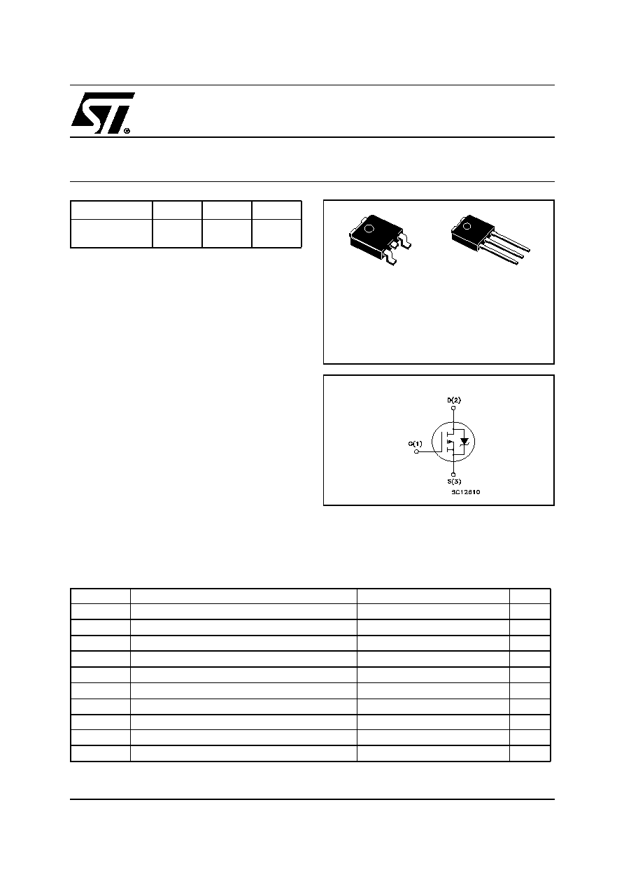
DPAK
1
3
3
2
1
IPAK
INTERNAL SCHEMATIC DIAGRAM

STD30PF03L - STD30PF03L-1
2/8
THERMAL DATA
AVALANCHE CHARACTERISTICS
ELECTRICAL CHARACTERISTICS (TCASE = 25 �C UNLESS OTHERWISE SPECIFIED)
OFF
ON
(1)
DYNAMIC
Rthj-case
Thermal Resistance Junction-case Max
2.14
�C/W
Rthj-amb
Thermal Resistance Junction-ambient Max
100
�C/W
T
j
Maximum Operating Junction Temperature
275
�C
Symbol
Parameter
Max Value
Unit
I
AR
Avalanche Current, Repetitive or Not-Repetitive
(pulse width limited by T
j
max)
24
A
E
AS
Single Pulse Avalanche Energy
(starting T
j
= 25 �C, I
D
= I
AR
, V
DD
= 25 V)
350
mJ
Symbol
Parameter
Test Conditions
Min.
Typ.
Max.
Unit
V
(BR)DSS
Drain-source
Breakdown Voltage
I
D
= 250 �A, V
GS
= 0
30
V
I
DSS
Zero Gate Voltage
Drain Current (V
GS
= 0)
V
DS
= Max Rating
1
�A
V
DS
= Max Rating, T
C
= 125 �C
10
�A
I
GSS
Gate-body Leakage
Current (V
DS
= 0)
V
GS
= � 16 V
�100
nA
Symbol
Parameter
Test Conditions
Min.
Typ.
Max.
Unit
V
GS(th)
Gate Threshold Voltage
V
DS
= V
GS
, I
D
= 250�A
1
V
R
DS(on)
Static Drain-source On
Resistance
V
GS
= 10 V, I
D
= 12 A
0025
0.028
V
GS
= 5 V, I
D
= 12 A
0.032
0.040
Symbol
Parameter
Test Conditions
Min.
Typ.
Max.
Unit
g
fs
(1)
Forward Transconductance
V
DS
= 15 V
,
I
D
= 12 A
23
S
C
iss
Input Capacitance
V
DS
= 25V, f = 1 MHz, V
GS
= 0
1670
pF
C
oss
Output Capacitance
345
pF
C
rss
Reverse Transfer
Capacitance
120
pF

3/8
STD30PF03L - STD30PF03L-1
ELECTRICAL CHARACTERISTICS (CONTINUED)
SWITCHING ON
SWITCHING OFF
SOURCE DRAIN DIODE
Note: 1. Pulsed: Pulse duration = 300 �s, duty cycle 1.5 %.
2. Pulse width limited by safe operating area.
Symbol
Parameter
Test Conditions
Min.
Typ.
Max.
Unit
t
d(on)
Turn-on Delay Time
V
DD
= 24 V, I
D
= 24 A
R
G
= 4.7
V
GS
= 4.5V
(see test circuit, Figure 3)
64
ns
t
r
Rise Time
122
ns
Q
g
Q
gs
Q
gd
Total Gate Charge
Gate-Source Charge
Gate-Drain Charge
V
DD
= 15 V, I
D
= 24 A,
V
GS
= 5 V
18.5
5.5
11
25
nC
nC
nC
Symbol
Parameter
Test Conditions
Min.
Typ.
Max.
Unit
t
d(off)
t
f
Turn-off-Delay Time
Fall Time
V
DD
= 24 V, I
D
= 24 A,
R
G
= 4.7
,
V
GS
= 4.5V
(see test circuit, Figure 3)
36
26
ns
ns
Symbol
Parameter
Test Conditions
Min.
Typ.
Max.
Unit
I
SD
Source-drain Current
24
A
I
SDM
(2)
Source-drain Current (pulsed)
96
A
V
SD
(1)
Forward On Voltage
I
SD
= 24 A, V
GS
= 0
2.3
V
t
rr
Q
rr
I
RRM
Reverse Recovery Time
Reverse Recovery Charge
Reverse Recovery Current
I
SD
= 24 A, di/dt = 100 A/�s,
V
DD
= 24 V, T
j
= 150 �C
(see test circuit, Figure 5)
40
52
2.6
ns
�
C
A

STD30PF03L - STD30PF03L-1
4/8
Fig. 5: Test Circuit For Inductive Load Switching
And Diode Recovery Times
Fig. 4: Gate Charge test Circuit
Fig. 2: Unclamped Inductive Waveform
Fig. 1: Unclamped Inductive Load Test Circuit
Fig. 3: Switching Times Test Circuit For
Resistive Load

5/8
STD30PF03L - STD30PF03L-1
DIM.
mm
inch
MIN.
TYP.
MAX.
MIN.
TYP.
MAX.
A
2.20
2.40
0.087
0.094
A1
0.90
1.10
0.035
0.043
A2
0.03
0.23
0.001
0.009
B
0.64
0.90
0.025
0.035
B2
5.20
5.40
0.204
0.213
C
0.45
0.60
0.018
0.024
C2
0.48
0.60
0.019
0.024
D
6.00
6.20
0.236
0.244
E
6.40
6.60
0.252
0.260
G
4.40
4.60
0.173
0.181
H
9.35
10.10
0.368
0.398
L2
0.8
0.031
L4
0.60
1.00
0.024
0.039
V2
0
o
8
o
0
o
0
o
P032P_B
TO-252 (DPAK) MECHANICAL DATA