
STD5NE10L
N - CHANNEL 100V - 0.3
- 5A - DPAK/IPAK
STripFET
TM
POWER MOSFET
PRELIMINARY DATA
s
TYPICAL R
DS(on)
= 0.3
s
EXCEPTIONAL dv/dt CAPABILITY
s
AVALANCHE RUGGED TECHNOLOGY
s
100 % AVALANCHE TESTED
s
APPLICATION ORIENTED
CHARACTERIZATION
s
FOR TAPE & REEL AND OTHER
PACKAGING OPTIONS CONTACT SALES
OFFICES
DESCRIPTION
This Power MOSFET is the latest development of
STMicroelectronics unique "
Single Feature
Size
TM
" strip-based process. The resulting tran-
sistor shows extremely high packing density for
low on-resistance, rugged avalanche charac-
teristics and less critical alignment steps therefore
a remarkable manufacturing reproducibility.
APPLICATIONS
s
DC MOTOR CONTROL (DISK DRIVES,etc.)
s
DC-DC & DC-AC CONVERTERS
s
SYNCHRONOUS RECTIFICATION
�
INTERNAL SCHEMATIC DIAGRAM
TYPE
V
DSS
R
DS(on)
I
D
STD5NE10L
100 V
< 0.4
5 A
October 1998
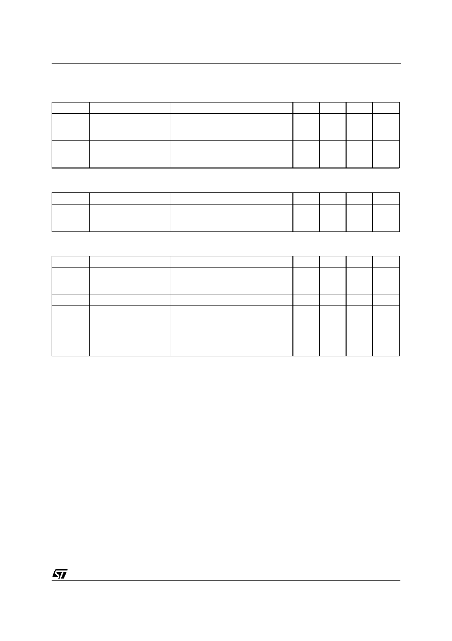
ABSOLUTE MAXIMUM RATINGS
Symb ol
Parameter
Value
Unit
V
DS
Drain-source Voltage (V
GS
= 0)
100
V
V
DGR
Drain- gate Volt age (R
G S
= 20 k
)
100
V
V
G S
Gat e-source Voltage
�
20
V
I
D
Drain Current (continuous) at T
c
= 25
o
C
5
A
I
D
Drain Current (continuous) at T
c
= 100
o
C
3.5
A
I
DM
(
�
)
Drain Current (pulsed)
20
A
P
tot
Tot al Dissipat ion at T
c
= 25
o
C
25
W
Derating F actor
0.2
W /
o
C
dv/ dt(
1
)
Peak Diode Recovery voltage slope
6
V/ns
T
st g
Storage Temperature
-65 to 150
o
C
T
j
Max. Operat ing Junction T emperature
150
o
C
(
�
) Pulse width limited by safe operating area
(
1
) I
SD
5 A, di/dt
200 A/
�
s, V
DD
V
(BR)DSS
, T
j
T
JMAX
1
3
DPAK
TO-252
(Suffix "T4")
3
2
1
IPAK
TO-251
(Suffix "-1")
1/5

THERMAL DATA
R
thj -case
R
thj -amb
R
thc-sink
T
l
Thermal Resistance Junction-case
Max
Thermal Resistance Junction-ambient
Max
Thermal Resistance Case-sink
Typ
Maximum Lead Temperature F or Soldering Purpose
5
100
1. 5
275
o
C/W
o
C/W
o
C/W
o
C
AVALANCHE CHARACTERISTICS
Symbo l
Parameter
Max Valu e
Unit
I
AR
Avalanche Current , Repet itive or Not-Repet itive
(pulse width limited by T
j
max)
5
A
E
AS
Single Pulse Avalanche Energy
(starting T
j
= 25
o
C, I
D
= I
AR
, V
DD
= 30 V)
20
mJ
ELECTRICAL CHARACTERISTICS (T
case
= 25
o
C unless otherwise specified)
OFF
Symbo l
Parameter
Test Con ditions
Min.
T yp.
Max.
Unit
V
(BR)DSS
Drain-source
Breakdown Voltage
I
D
= 250
�
A
V
GS
= 0
100
V
I
DSS
Zero G ate Voltage
Drain Current (V
GS
= 0)
V
DS
= Max Rating
V
DS
= Max Rating
T
c
= 100
o
C
1
10
�
A
�
A
I
G SS
Gat e-body Leakage
Current (V
DS
= 0)
V
GS
=
�
20 V
�
100
nA
ON (
)
Symbo l
Parameter
Test Con ditions
Min.
T yp.
Max.
Unit
V
G S(th)
Gat e Threshold
Voltage
V
DS
= V
GS
I
D
= 250
�
A
1
1.7
2. 5
V
R
DS(on)
Static Drain-source O n
Resist ance
V
GS
= 10 V I
D
= 2.5 A
V
GS
= 5 V I
D
= 2. 5 A
0.3
0.35
0. 4
0.45
I
D(o n)
On Stat e Drain Current
V
DS
> I
D(o n)
x R
DS(on )ma x
V
GS
= 10 V
5
A
DYNAMIC
Symbo l
Parameter
Test Con ditions
Min.
T yp.
Max.
Unit
g
f s
(
)
Forward
Transconduct ance
V
DS
> I
D(o n)
x R
DS(on )ma x
I
D
=2.5 A
2
S
C
iss
C
os s
C
rss
Input Capacitance
Out put Capacitance
Reverse T ransfer
Capacitance
V
DS
= 25 V
f = 1 MHz
V
GS
= 0
345
45
20
450
60
25
pF
pF
pF
STD5NE10L
2/5
ELECTRICAL CHARACTERISTICS (continued)
SWITCHING ON
Symbo l
Parameter
Test Con ditions
Min.
T yp.
Max.
Unit
t
d(on)
t
r
Turn-on Time
Rise Time
V
DD
= 50 V
I
D
= 2. 5 A
R
G
= 4.7
V
GS
= 5 V
7
17
9
22
ns
ns
Q
g
Q
gs
Q
gd
Tot al Gate Charge
Gat e-Source Charge
Gat e-Drain Charge
V
DD
= 80 V
I
D
= 5 A
V
GS
= 5 V
10
5
4
14
nC
nC
nC
SWITCHING OFF
Symbo l
Parameter
Test Con ditions
Min.
T yp.
Max.
Unit
t
r (Voff)
t
f
t
c
Off -volt age Rise Time
Fall Time
Cross-over Time
V
DD
= 80 V
I
D
= 5 A
R
G
= 4.7
V
GS
= 10 V
8
9
19
10
12
25
ns
ns
ns
SOURCE DRAIN DIODE
Symbo l
Parameter
Test Con ditions
Min.
T yp.
Max.
Unit
I
SD
I
SDM
(
�
)
Source-drain Current
Source-drain Current
(pulsed)
5
20
A
A
V
SD
(
)
Forward On Volt age
I
SD
= 8 A
V
GS
= 0
1. 5
V
t
rr
Q
rr
I
RRM
Reverse Recovery
Time
Reverse Recovery
Charge
Reverse Recovery
Current
I
SD
= 5 A
di/dt = 100 A/
�
s
V
DD
= 30 V
T
j
= 150
o
C
75
190
5
ns
�
C
A
(
) Pulsed: Pulse duration = 300
�
s, duty cycle 1.5 %
(
�
) Pulse width limited by safe operating area
STD5NE10L
3/5

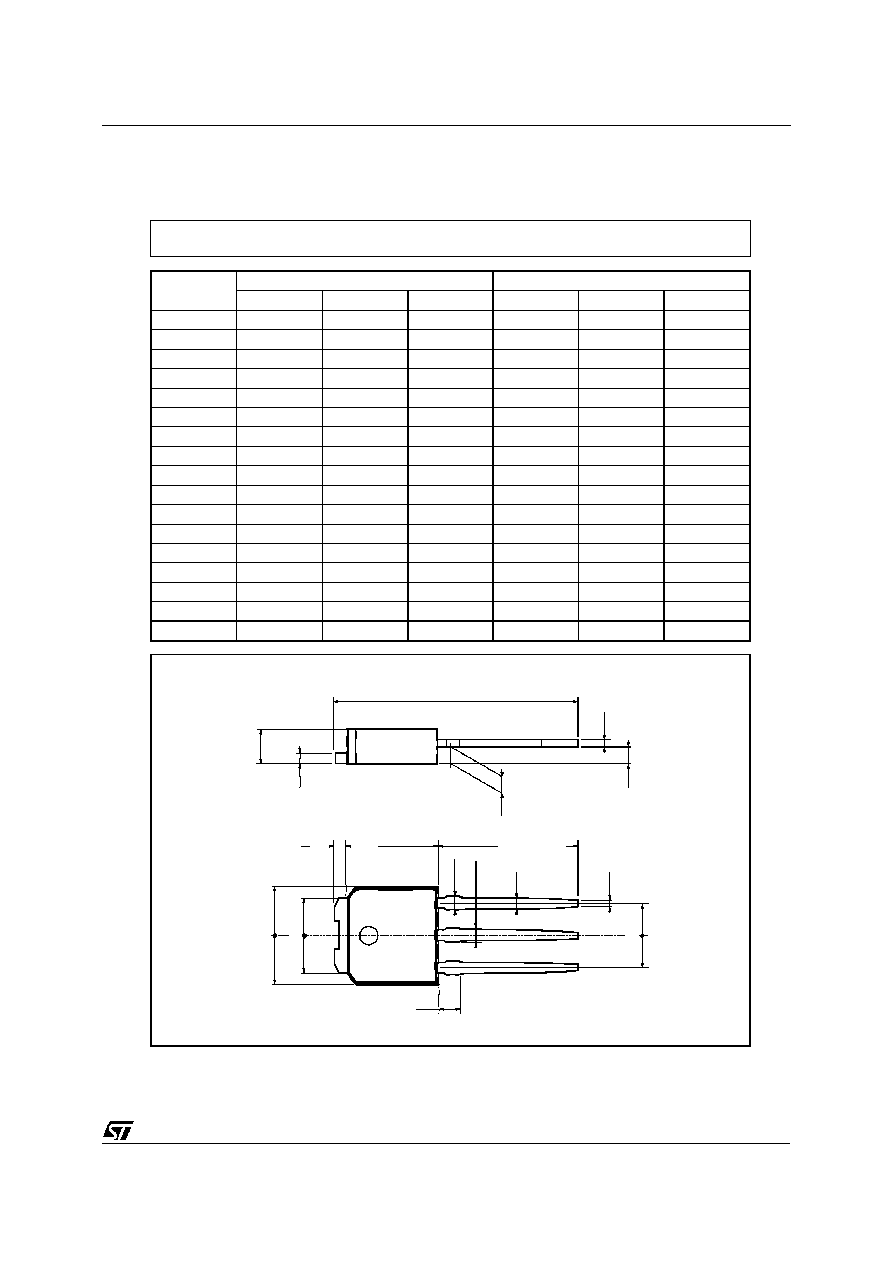
DIM.
mm
inch
MIN.
TYP.
MAX.
MIN.
TYP.
MAX.
A
2.2
2.4
0.086
0.094
A1
0.9
1.1
0.035
0.043
A2
0.03
0.23
0.001
0.009
B
0.64
0.9
0.025
0.035
B2
5.2
5.4
0.204
0.212
C
0.45
0.6
0.017
0.023
C2
0.48
0.6
0.019
0.023
D
6
6.2
0.236
0.244
E
6.4
6.6
0.252
0.260
G
4.4
4.6
0.173
0.181
H
9.35
10.1
0.368
0.397
L2
0.8
0.031
L4
0.6
1
0.023
0.039
==
D
L2
L4
13
==
B
E
==
B2
G
2
A
C2
C
H
A1
DETAIL "A"
A2
DETAIL "A"
TO-252 (DPAK) MECHANICAL DATA
0068772-B
STD5NE10L
4/5
DIM.
mm
inch
MIN.
TYP.
MAX.
MIN.
TYP.
MAX.
A
2.2
2.4
0.086
0.094
A1
0.9
1.1
0.035
0.043
A3
0.7
1.3
0.027
0.051
B
0.64
0.9
0.025
0.031
B2
5.2
5.4
0.204
0.212
B3
0.85
0.033
B5
0.3
0.012
B6
0.95
0.037
C
0.45
0.6
0.017
0.023
C2
0.48
0.6
0.019
0.023
D
6
6.2
0.236
0.244
E
6.4
6.6
0.252
0.260
G
4.4
4.6
0.173
0.181
H
15.9
16.3
0.626
0.641
L
9
9.4
0.354
0.370
L1
0.8
1.2
0.031
0.047
L2
0.8
1
0.031
0.039
A
C2
C
A3
H
A1
D
L
L2
L1
13
==
B3
B
B6
B2
E
G
==
==
B5
2
TO-251 (IPAK) MECHANICAL DATA
0068771-E
STD5NE10L
5/5