1/11
September 2004
STD95NH02L
N-CHANNEL 24V - 0.0039
- 80A DPAK
ULTRA LOW GATE CHARGE STripFETTM MOSFET
Table 1: General Features
s
TYPICAL R
DS
(on) = 0.0039
@ 10 V
s
CONDUCTION LOSSES REDUCED
s
SWITCHING LOSSES REDUCED
DESCRIPTION
The STD95NH02L is based on the latest genera-
tion of ST's proprietary STripFETTM technology. An
innovative layout enables the device to also exhibit
extremely low gate charge for the most demanding
requirements in high-frequency DC-DC convert-
ers. It's therefore ideal for high-density converters
in Telecom and Computer applications.
APPLICATIONS
s
SPECIFICALLY DESIGNED AND OPTIMISED
FOR HIGH EFFICIENCY DC/DC
CONVERTERS
Table 2: Order Codes
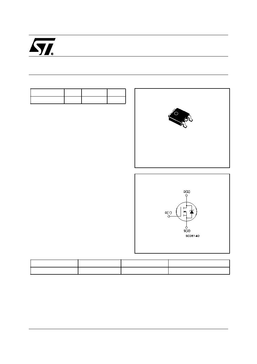
Figure 1: Package
Figure 2: Internal Schematic Diagram
TYPE
V
DSS
R
DS(on)
I
D
STD95NH02L
24 V
< 0.005
80(*) A
DPAK
1
3
TO-252
(Suffix "T4")
PART NUMBER
MARKING
PACKAGE
PACKAGING
STD95NH02LT4
D95NH02L
DPAK
TAPE & REEL
Rev. 2

STD95NH02L
2/11
Table 3: Absolute Maximum ratings
(1) Garanted when external R
g
= 4.7
and t
f
< t
f
max.
(2) Pulse width limited by safe operating area.
(3) Starting T
j
= 25∞C, I
D
= 40A, V
DD
= 22V
(*) Value limited by wires
Table 4: Thermal Data
ELECTRICAL CHARACTERISTICS (T
CASE
=25∞C UNLESS OTHERWISE SPECIFIED)
Table 5: On/Off
Symbol
Parameter
Value
Unit
V
spike
(1)
Drain-source Voltage Rating
30
V
V
DS
Drain-source Voltage (V
GS
= 0)
24
V
V
DGR
Drain-gate Voltage (R
GS
= 20 k
)
24
V
V
GS
Gate- source Voltage
± 20
V
I
D
(*)
Drain Current (continuous) at T
C
= 25∞C
80
A
I
D
Drain Current (continuous) at T
C
= 100∞C
68
A
I
DM
(2)
Drain Current (pulsed)
320
A
P
TOT
Total Dissipation at T
C
= 25∞C
100
W
Derating Factor
0.67
W/∞C
E
AS
(3)
Single Pulse Avalanche Energy
600
mJ
T
stg
Storage Temperature
-55 to 175
∞C
T
j
Max. Operating Junction Temperature
Rthj-case
Thermal Resistance Junction-case Max
1.5
∞C/W
Rthj-amb
Thermal Resistance Junction-ambient Max
100
∞C/W
T
l
Maximum Lead Temperature For Soldering
Purpose
275
∞C
Symbol
Parameter
Test Conditions
Min.
Typ.
Max.
Unit
V
(BR)DSS
Drain-source
Breakdown Voltage
I
D
= 250 µA, V
GS
= 0
24
V
I
DSS
Zero Gate Voltage
Drain Current (V
GS
= 0)
V
DS
= Max Rating
V
DS
= Max Rating, T
C
= 125 ∞C
1
10
µA
µA
I
GSS
Gate-body Leakage
Current (V
DS
= 0)
V
GS
= ± 20V
±100
nA
V
GS(th)
Gate Threshold Voltage
V
DS
= V
GS
, I
D
= 250µA
1
V
R
DS(on)
Static Drain-source On
Resistance
V
GS
= 10 V, I
D
= 40 A
V
GS
= 5 V, I
D
=40 A
0.0039
0.0055
0.005
0.009

3/11
STD95NH02L
ELECTRICAL CHARACTERISTICS (CONTINUED)
Table 6: Dynamic
Table 7: Source Drain Diode
(4). Pulsed: Pulse duration = 300 µs, duty cycle 1.5 %.
(5). Q
oss
= C
oss
*
V
in
, C
oss
= C
gd
+C
ds
. See Appendix A.
(6). Gate charge for Syncronous Operation.
Symbol
Parameter
Test Conditions
Min.
Typ.
Max.
Unit
g
fs
(4)
Forward Transconductance
V
DS
= 10 V
,
I
D
= 10 A
30
S
C
iss
C
oss
C
rss
Input Capacitance
Output Capacitance
Reverse Transfer
Capacitance
V
DS
= 15V, f = 1 MHz, V
GS
= 0
2070
990
90
pF
pF
pF
t
d(on)
t
r
t
d(off)
t
f
Turn-on Delay Time
Rise Time
Turn-off Delay Time
Fall Time
V
DD
= 12 V, I
D
= 40 A,
R
G
= 4.7
V
GS
= 10 V
(see Figure 16)
20
110
47
20
ns
ns
ns
ns
Q
g
Q
gs
Q
gd
Total Gate Charge
Gate-Source Charge
Gate-Drain Charge
V
DD
=
12 V, I
D
= 80 A,
V
GS
= 5 V
(see Figure 19)
17
7.6
6.8
nC
nC
nC
Q
oss
(5)
Output Charge
V
DS
= 19 V, V
GS
= 0 V
22.6
nC
Q
gls
(6)
Third-Quadrant Gate Charge
V
DS
< 0 V, V
GS
= 5 V
15
nC
R
G
Gate Input Resistance
f = 1 MHz Gate DC Bias = 0
Test Signal Level = 20 mV
Open Drain
1.8
Symbol
Parameter
Test Conditions
Min.
Typ.
Max.
Unit
I
SD
Source-drain Current
80
A
I
SDM
Source-drain Current (pulsed)
320
A
V
SD
(4)
Forward On Voltage
I
SD
= 40A, V
GS
= 0
1.3
V
t
rr
Q
rr
I
RRM
Reverse Recovery Time
Reverse Recovery Charge
Reverse Recovery Current
I
SD
= 80A, di/dt = 100 A/µs,
V
DD
=20 V, T
j
= 150∞C
(see Figure 16)
42
50.4
2.4
ns
nC
A
STD95NH02L
4/11
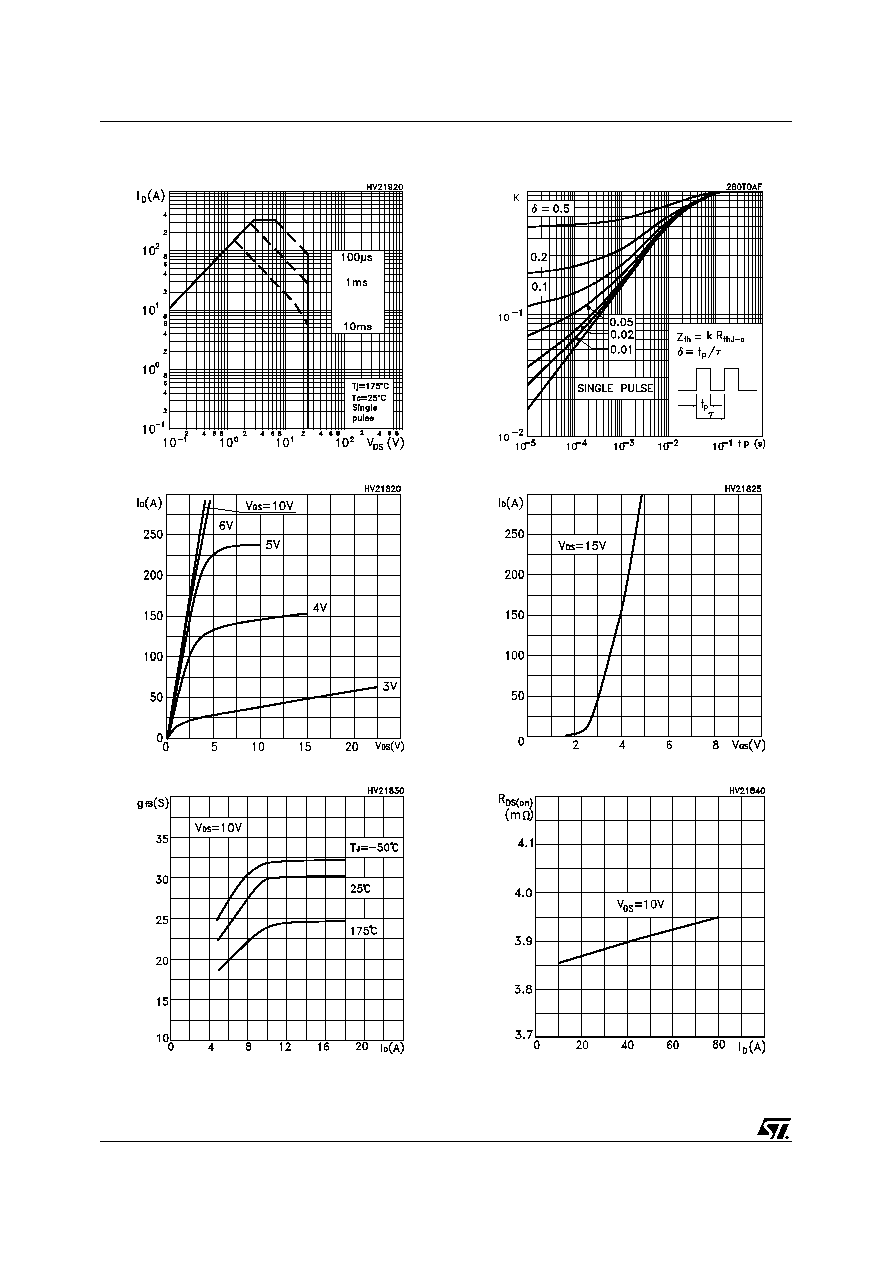
Figure 3: Safe Operating Area
Figure 4: Output Characteristics
Figure 5: Transconductance
Figure 6: Thermal Impedance
Figure 7: Transfer Characteristics
Figure 8: Static Drain-source On Resistance

5/11
STD95NH02L
Figure 9: Gate Charge vs Gate-source Voltage
Figure 10: Normalized Gate Thereshold Volt-
age vs Temperature
Figure 11: Dource-Drain Diode Forward Char-
acteristics
Figure 12: Capacitance Variations
Figure 13: Normalized On Resistance vs Tem-
perature
Figure 14: Normalized Breakdown Voltage vs
Temperature