1/16
October 2005
STP21NM50N-STF21NM50N-STW21NM50N
STB21NM50N - STB21NM50N-1
N-CHANNEL 500V - 0.15
- 18A TO-220/FP/D
2
/I
2
PAK/TO-247
SECOND GENERATION MDmeshTM MOSFET
Table 1: General Features
100% AVALANCHE TESTED
LOW INPUT CAPACITANCE AND GATE
CHARGE
LOW GATE INPUT RESISTANCE
DESCRIPTION
The STx21NM50N is realized with the second
generation of MDmesh Technology. This revolu-
tionary MOSFET associates a new vertical struc-
ture to the Company's strip layout to yield one of
the world's lowest on-resistance and gate charge.
It is therefore suitable for the most demanding high
efficiency converters
APPLICATIONS
The MDmeshTM II family is very suitable for in-
creasing power density of high voltage converters
allowing system miniaturization and higher effi-
ciencies.
Table 2: Order Codes
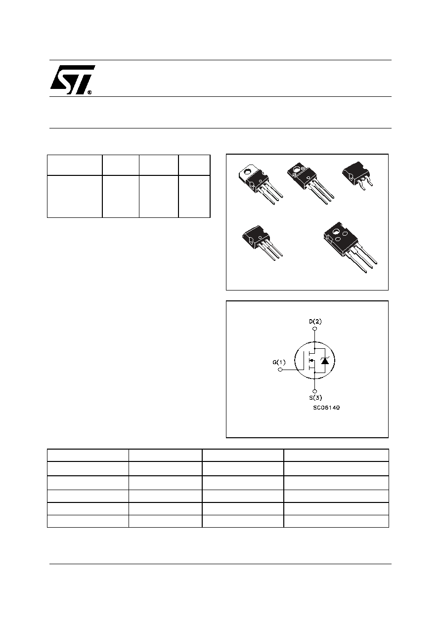
Figure 1: Package
Figure 2: Internal Schematic Diagram
TYPE
V
DSS
(@Tjmax)
R
DS(on)
I
D
STB21NM50N
STB21NM50N-1
STF21NM50N
STP21NM50N
STW21NM50N
550 V
550 V
550 V
550 V
550 V
< 0.19
< 0.19
< 0.19
< 0.19
< 0.19
18 A
18 A
18 A (*)
18 A
18 A
1
2
3
TO-220
D
2
PAK
1
2
3
TO-220FP
1
3
1
2
3
I
2
PAK
1
2
3
TO-247
SALES TYPE
MARKING
PACKAGE
PACKAGING
STB21NM50N
B21NM50N
D
2
PAK
TAPE & REEL
STB21NM50N-1
B21NM50N
I
2
PAK
TUBE
STF21NM50N
F21NM50N
TO-220FP
TUBE
STP21NM50N
P21NM50N
TO-220
TUBE
STW21NM50N
W21NM50N
TO-247
TUBE
Rev. 3
STP21NM50N - STF21NM50N - STB21NM50N - STB21NM50N-1 - STW21NM50N
2/16
Table 3: Absolute Maximum ratings
( )
Pulse width limited by safe operating area
(*) Limited only by maximum temperature allowed
(1) I
SD
18 A, di/dt
400 A/µs, V
DD
=80%
V
(BR)DSS
Table 4: Thermal Data
Table 5: Avalanche Characteristics
Symbol
Parameter
Value
Unit
TO-220 / D
2
PAK / I
2
PAK
/ TO-247
TO-220FP
V
DS
Drain-source Voltage (V
GS
= 0)
500
V
V
DGR
Drain-gate Voltage (R
GS
= 20 k
)
500
V
V
GS
Gate- source Voltage
±25
V
I
D
Drain Current (continuous) at T
C
= 25∞C
18
18 (*)
A
I
D
Drain Current (continuous) at T
C
= 100∞C
11
11 (*)
A
I
DM
( )
Drain Current (pulsed)
72
72 (*)
A
P
TOT
Total Dissipation at T
C
= 25∞C
140
30
W
Derating Factor
1.12
0.23
W/∞C
dv/dt(1)
Peak Diode Recovery voltage slope
15
V/ns
Viso
Insulation Winthstand Voltage (DC)
--
2500
V
T
stg
Storage Temperature
≠55 to 150
150
∞C
T
j
Max. Operating Junction Temperature
TO-220 / D≤PAK / I≤PAK
/ TO-247
TO-220FP
Rthj-case
Thermal Resistance Junction-case Max
0.89
4.21
∞C/W
Rthj-amb
Thermal Resistance Junction-ambient Max
62.5
∞C/W
T
l
Maximum Lead Temperature For Soldering
Purpose
300
∞C
Symbol
Parameter
Max Value
Unit
I
AS
Avalanche Current, Repetitive or Not-Repetitive
(pulse width limited by T
j
max)
9
A
E
AS
Single Pulse Avalanche Energy
(starting T
j
= 25 ∞C, I
D
= I
AR
, V
DD
= 50 V)
480
mJ

3/16
STP21NM50N - STF21NM50N - STB21NM50N - STB21NM50N-1 - STW21NM50N
ELECTRICAL CHARACTERISTICS (T
CASE
=25∞C UNLESS OTHERWISE SPECIFIED)
Table 6: On/Off
(2) Characteristic value at turn off on inductive load
Table 7: Dynamic
(*) C
oss eq.
is defined as a constant equivalent capacitance giving the same charging time as C
oss
when V
DS
increases from 0 to 80% V
DSS
Table 8: Source Drain Diode
Note: 1. Pulsed: Pulse duration = 300 µs, duty cycle 1.5 %.
Symbol
Parameter
Test Conditions
Value
Unit
Min.
Typ.
Max.
V
(BR)DSS
Drain-source
Breakdown Voltage
I
D
= 1mA, V
GS
= 0
500
V
dv/dt(2)
Drain Source Voltage
Slope
Vdd=400V, Id=25A, Vgs=10V
44
V/ns
I
DSS
Zero Gate Voltage
Drain Current (V
GS
= 0)
V
DS
= Max Rating
V
DS
= Max Rating
T
C
= 125 ∞C
1
10
µA
µA
I
GSS
Gate-body Leakage
Current (V
DS
= 0)
V
GS
= ± 20V
100
nA
V
GS(th)
Gate Threshold Voltage
V
DS
= V
GS
, I
D
= 250 µA
2
3
4
V
R
DS(on)
Static Drain-source On
Resistance
V
GS
= 10V, I
D
= 9 A
0.150
0.190
Symbol
Parameter
Test Conditions
Min.
Typ.
Max.
Unit
g
fs
(1)
Forward Transconductance
V
DS
= 15 V
,
I
D
= 9 A
12
S
C
iss
C
oss
C
rss
Input Capacitance
Output Capacitance
Reverse Transfer
Capacitance
V
DS
= 25V, f = 1 MHz, V
GS
= 0
1950
420
60
pF
pF
pF
C
oss eq.
(*)
Equivalent Output
Capacitance
V
GS
= 0V, V
DS
= 0V to 400V
270
pF
t
d(on)
t
r
t
d(off)
t
f
Turn-on Delay Time
Rise Time
Off-voltageRise Time
Fall Time
V
DD
=250 V, I
D
= 9 A
R
G
= 4.7
V
GS
= 10 V
(see Figure 18)
22
18
90
30
ns
ns
ns
ns
Q
g
Q
gs
Q
gd
Total Gate Charge
Gate-Source Charge
Gate-Drain Charge
V
DD
= 400V, I
D
= 18 A,
V
GS
= 10V,
(see Figure 21)
65
10
30
nC
nC
nC
R
g
Gate Input Resistance
f=1MHz Gate DC Bias=0
Test Signal Level=20mV
Open Drain
1.6
Symbol
Parameter
Test Conditions
Min.
Typ.
Max.
Unit
I
SD
I
SDM
Source-drain Current
Source-drain Current (pulsed)
18
72
A
A
V
SD
(1)
Forward On Voltage
I
SD
= 18 A, V
GS
= 0
1.5
V
t
rr
Q
rr
I
RRM
Reverse Recovery Time
Reverse Recovery Charge
Reverse Recovery Current
I
SD
= 18 A, di/dt = 100 A/µs
V
DD
= 100 V, T
j
= 25∞C
(see Figure 19)
360
5
27
ns
µC
A
t
rr
Q
rr
I
RRM
Reverse Recovery Time
Reverse Recovery Charge
Reverse Recovery Current
I
SD
= 18A, di/dt = 100 A/µs
V
DD
= 100 V, T
j
= 150∞C
(see Figure 19)
640
6.5
27
ns
µC
A
STP21NM50N - STF21NM50N - STB21NM50N - STB21NM50N-1 - STW21NM50N
4/16
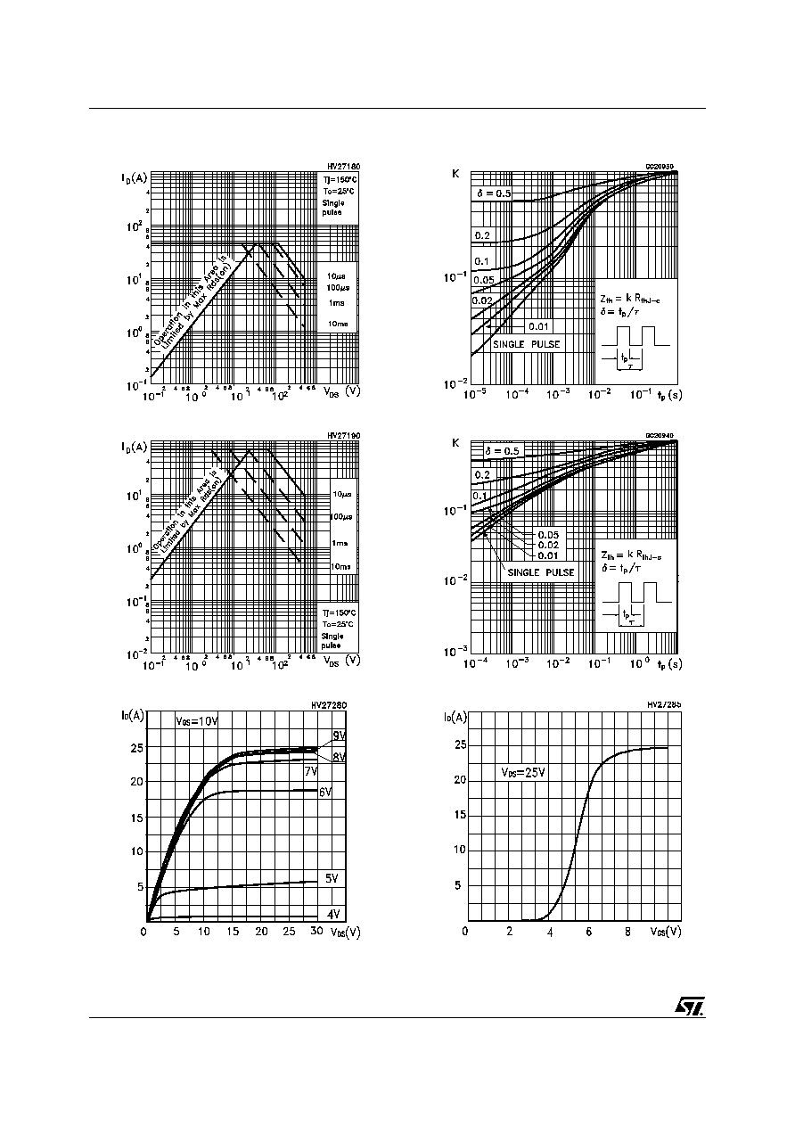
Figure 3: Safe Operating Area For TO-220
Figure 4: Safe Operating Area For TO-220FP
Figure 5: Output Characteristics
Figure 6: Thermal Impedance For TO-220
Figure 7: Thermal Impedance For TO-220FP
Figure 8: Transfer Characteristics
5/16
STP21NM50N - STF21NM50N - STB21NM50N - STB21NM50N-1 - STW21NM50N
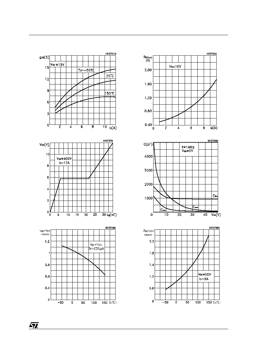
Figure 9: Transconductance
Figure 10: Gate Charge vs Gate-source Voltage
Figure 11: Normalized Gate Threshold Voltage
vs Temperature
Figure 12: Static Drain-source On Resistance
Figure 13: Capacitance Variations
Figure 14: Normalized On Resistance vs Tem-
perature