
STGP7NB60HD
STGP7NB60HDFP
N-CHANNEL 7A - 600V TO-220/FP
PowerMESH
TM
IGBT
s
HIGH INPUT IMPEDANCE
(VOLTAGE DRIVEN)
s
LOW ON-VOLTAGE DROP (V
cesat
)
s
LOW GATE CHARGE
s
HIGH CURRENT CAPABILITY
s
VERY HIGH FREQUENCY OPERATION
s
OFF LOSSES INCLUDE TAIL CURRENT
s
CO-PACKAGED WITH TURBOSWITCH
TM
ANTIPARALLEL DIODE
DESCRIPTION
Using the latest high voltage technology based
on a patented strip layout, STMicroelectronics
has designed an advanced family of IGBTs, the
PowerMESH
TM
IGBTs,
with
outstanding
perfomances. The suffix "H" identifies a family
optimized to achieve very low switching times for
high frequency applications (<120kHz).
APPLICATIONS
s
HIGH FREQUENCY MOTOR CONTROLS
s
SMPS AND PFC IN BOTH HARD SWITCH
AND RESONANT TOPOLOGIES
Æ
INTERNAL SCHEMATIC DIAGRAM
TYPE
V
CES
V
CE(sat)
I
C
STGP7NB60HD
STGP7NB60HDFP
600 V
600 V
< 2. 8 V
< 2. 8 V
7 A
7 A
June 1999
1
2
3
TO-220
TO-220FP
1
2
3
ABSOLUTE MAXIMUM RATINGS
Symbol
Parameter
Value
Unit
STGP7NB60HD
ST GP7NB60HDFP
V
CES
Collector-Emitter Voltage (VGS = 0)
600
600
V
V
GE
G ate-Emitter Voltage
±
20
±
20
V
I
C
Collector Current (continuous) at Tc = 25
o
C
14
13
A
I
C
Collector Current (continuous) at Tc = 100
o
C
7
6
A
I
CM
(
∑
)
Collector Current (pulsed)
56
56
A
P
tot
T otal Dissipation at T c = 25
o
C
80
35
W
Derating Factor
0.64
0.28
W /
o
C
T
s tg
Storage T emperature
-65 t o 150
o
C
T
j
Max. O perat ing Junct ion T emperature
150
o
C
(
∑
) Pulse width limited by safe operating area
1/9

THERMAL DATA
TO-220
T O-220FP
R
thj -case
Thermal Resistance Junction-case
Max
1.56
3.57
o
C/W
R
thj -amb
R
thc-sink
Thermal Resistance Junction-ambient
Max
Thermal Resistance Case-sink
T yp
62.5
0.5
o
C/W
o
C/W
ELECTRICAL CHARACTERISTICS (T
j
= 25
o
C unless otherwise specified)
OFF
Symbol
Parameter
Test Conditions
Min.
Typ.
Max.
Unit
V
BR(CES)
Collector-Emitt er
Breakdown Voltage
I
C
= 250
µ
A
V
GE
= 0
600
V
I
CES
Collector cut-of f
(V
G E
= 0)
V
CE
= Max Rat ing
T
j
=
25
o
C
V
CE
= Max Rat ing
T
j
= 125
o
C
250
2000
µ
A
µ
A
I
G ES
Gat e-Emitter Leakage
Current (V
CE
= 0)
V
GE
=
±
20 V
V
CE
= 0
±
100
nA
ON (
)
Symbol
Parameter
Test Conditions
Min.
Typ.
Max.
Unit
V
G E(th)
Gat e Threshold
Voltage
V
CE
= V
GE
I
C
= 250
µ
A
3
5
V
V
CE(SAT )
Collector-Emitt er
Sat uration Voltage
V
GE
= 15 V
I
C
= 7 A
V
GE
= 15 V
I
C
= 7 A
T
j
= 125
o
C
2.3
1.9
2. 8
V
V
DYNAMIC
Symbol
Parameter
Test Conditions
Min.
Typ.
Max.
Unit
g
f s
Forward
Transconductance
V
CE
=25 V
I
C
= 7 A
3. 5
5
S
C
i es
C
o es
C
res
Input Capacitance
Out put Capacitance
Reverse Transfer
Capacitance
V
CE
= 25 V
f = 1 MHz
V
GE
= 0
390
45
10
560
68
15
730
90
20
pF
pF
pF
Q
G
Q
GE
Q
G C
Tot al G ate Charge
Gat e-Emitter Charge
Gat e-Collector Charge
V
CE
= 480 V
I
C
= 7 A
V
GE
= 15 V
42
7.9
17.6
55
nC
nC
nC
I
CL
Lat ching Current
V
clamp
= 480 V
R
G
=10
T
j
= 150
o
C
28
A
SWITCHING ON
Symbol
Parameter
Test Conditions
Min.
Typ.
Max.
Unit
t
d(on)
t
r
Delay Time
Rise Time
V
CC
= 480 V
I
C
= 7 A
V
GE
= 15 V
R
G
= 10
15
48
ns
ns
(di/dt)
on
E
o n
(
r
)
Turn-on Current Slope
Turn-on
Switching Losses
V
CC
= 480 V
I
C
= 7 A
R
G
= 10
V
GE
= 15 V
T
j
= 125
o
C
160
185
A/
µ
s
µ
J
STGP7NB60HD/FP
2/9

ELECTRICAL CHARACTERISTICS (continued)
SWITCHING OFF
Symbol
Parameter
Test Conditions
Min.
Typ.
Max.
Unit
t
c
t
r
(v
off
)
t
d
(
o ff
)
t
f
E
o ff
(**)
E
ts
(
r
)
Cross-O ver Time
Off Volt age Rise Time
Delay Time
Fall T ime
Turn-off Swit ching Loss
Tot al Switching Loss
V
CC
= 480 V
I
C
= 7 A
R
G E
= 10
V
GE
= 15 V
85
20
75
70
85
235
ns
ns
ns
ns
µ
J
µ
J
t
c
t
r
(v
off
)
t
d
(
o ff
)
t
f
E
o ff
(**)
E
ts
(
r
)
Cross-O ver Time
Off Volt age Rise Time
Delay Time
Fall T ime
Turn-off Swit ching Loss
Tot al Switching Loss
V
CC
= 480 V
I
C
= 7 A
R
G E
= 10
V
GE
= 15 V
T
j
= 125
o
C
150
50
110
110
220
405
ns
ns
ns
ns
µ
J
µ
J
COLLECTOR-EMITTER DIODE
Symbol
Parameter
T est Conditions
Min.
T yp.
Max.
Unit
I
f
I
fm
Forward Current
Forward Current pulsed
7
56
A
A
V
f
Forward On-Voltage
I
f
= 7 A
I
f
= 7 A
T
j
= 125
o
C
1.6
1.4
2.0
V
V
t
rr
Q
rr
I
rrm
Reverse Recovery Time
Reverse Recovery Charge
Reverse Recovery Current
I
f
= 7 A
V
R
=200 V
dI/dt = 100 A/
µ
S
T
j
= 125
o
C
100
180
3.6
ns
nC
A
(
∑
) Pulse width limited by max. junction temperature
(
r
) Include recovery lossess on the STTA506 freewheeling diode
(
) Pulsed: Pulse duration = 300
µ
s, duty cycle 1.5 %
(**)Losses Include Also The Tail (Jedec Standardization)
Thermal Impedeance For TO-220
Thermal Impedeance For TO-220FP
STGP7NB60HD/FP
3/9
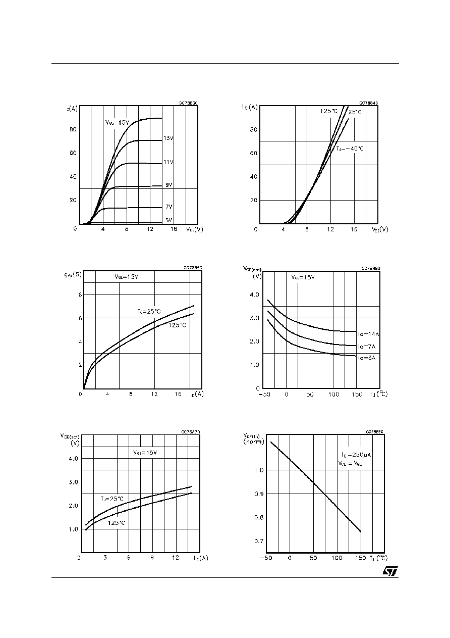
Output Characteristics
Transconductance
Collector-Emitter On Voltage vs Collector Current
Transfer Characteristics
Collector-Emitter On Voltage vs Temperature
Gate Threshold vs Temperature
STGP7NB60HD/FP
4/9

Normalized Breakdown Voltage vs Temperature
Gate Charge vs Gate-Emitter Voltage
Total Switching Losses vs Temperature
Capacitance Variations
Total Switching Losses vs Gate Resistance
Total Switching Losses vs Collector Current
STGP7NB60HD/FP
5/9