STW5NA90
STH5NA90FI
N - CHANNEL ENHANCEMENT MODE
POWER MOS TRANSISTORS
PRELIMINARY DATA
s
TYPICAL R
DS(on)
= 2.1
s
±
30 V GATE-TO-SOURCE VOLTAGE
RATING
s
100% AVALANCHE TESTED
s
REPETITIVE AVALANCHE DATA AT 100
o
C
s
GATE CHARGE MINIMISED
s
REDUCED THRESHOLD VOLTAGE SPREAD
APPLICATIONS
s
HIGH CURRENT, HIGH SPEED SWITCHING
s
SWITCH MODE POWER SUPPLY (SMPS)
s
DC-AC CONVERTERS FOR WELDING
EQUIPMENT AND UNINTERRUPTIBLE
POWER SUPPLIES AND MOTOR DRIVE
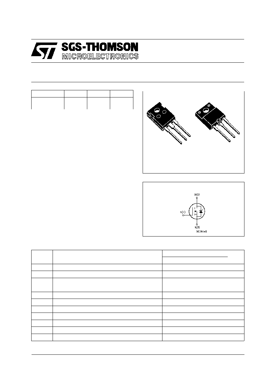
INTERNAL SCHEMATIC DIAGRAM
ABSOLUTE MAXIMUM RATINGS
Symbol
Parameter
Valu e
Un it
STW 5NA90
ST H5NA90F I
V
DS
Drain-source Voltage (V
GS
= 0)
900
V
V
DGR
Drain- gate Volt age (R
G S
= 20 k
)
900
V
V
GS
Gat e-source Voltage
±
30
V
I
D
Drain Current (continuous) at T
c
= 25
o
C
5. 3
3. 5
A
I
D
Drain Current (continuous) at T
c
= 100
o
C
3. 4
2. 2
A
I
DM
(
∑
)
Drain Current (pulsed)
21. 2
21.2
A
P
t ot
Tot al Dissipation at T
c
= 25
o
C
150
60
W
Derating Factor
1. 2
0.48
W /
o
C
V
ISO
Insulat ion W it hst and Voltage (DC)
4000
V
T
stg
Storage T emperat ure
-65 to 150
o
C
T
j
Max. O perating Junction T emperat ure
150
o
C
(
∑
) Pulse width limited by safe operating area
TYPE
V
DSS
R
DS(on)
I
D
ST W5NA90
ST H5NA90F I
900 V
900 V
< 2.5
< 2.5
5.3 A
3.5 A
January 1998
TO-247
ISOWATT218
1
2
3
1
2
3
1/6

THERMAL DATA
T O-247
ISOW ATT 218
R
t hj-ca se
Thermal Resistance Junction-case
Max
0. 83
2. 08
o
C/ W
R
t hj- amb
R
thc- si nk
T
l
Thermal Resistance Junction-ambient
Max
Thermal Resistance Case-sink
Typ
Maximum Lead Temperature For Soldering Purpose
30
0.1
300
o
C/ W
o
C/ W
o
C
AVALANCHE CHARACTERISTICS
Symb ol
Parameter
Max Valu e
Uni t
I
AR
Avalanche Current, Repetitive or Not -Repet itive
(pulse width limited by T
j
max,
< 1%)
5.3
A
E
AS
Single Pulse Avalanche Energy
(starting T
j
= 25
o
C, I
D
= I
AR
, V
DD
= 50 V)
520
mJ
ELECTRICAL CHARACTERISTICS (T
case
= 25
o
C unless otherwise specified)
OFF
Symb ol
Parameter
Test Cond ition s
Mi n.
Typ .
Max.
Un it
V
(BR)DSS
Drain-source
Breakdown Volt age
I
D
= 250
µ
A
V
GS
= 0
900
V
I
DSS
Zero G ate Voltage
Drain Current (V
GS
= 0)
V
DS
= Max Rating
V
DS
= Max Rating
T
c
= 100
o
C
25
250
µ
A
µ
A
I
GSS
Gate-body Leakage
Current (V
DS
= 0)
V
G S
=
±
30 V
±
100
nA
ON (
)
Symb ol
Parameter
Test Cond ition s
Mi n.
Typ .
Max.
Un it
V
GS(th)
Gate Threshold
Voltage
V
DS
= V
GS
I
D
= 250
µ
A
2.25
3
3.75
V
R
DS( on)
St atic Drain-source On
Resistance
V
G S
= 10V
I
D
= 2.5 A
V
G S
= 10V
I
D
= 2. 5 A
T
c
= 100
o
C
2.1
2.5
5
I
D(o n)
On St ate Drain Current
V
DS
> I
D(on)
x R
DS(on) max
V
G S
= 10 V
5. 3
A
DYNAMIC
Symb ol
Parameter
Test Cond ition s
Mi n.
Typ .
Max.
Un it
g
fs
(
)
Forward
Transconduct ance
V
DS
> I
D(on)
x R
DS(on) max
I
D
= 2.5 A
4
6.4
S
C
iss
C
oss
C
rss
Input Capacitance
Output Capacit ance
Reverse T ransfer
Capacitance
V
DS
= 25 V
f = 1 MHz
V
GS
= 0
1350
150
40
1900
210
60
pF
pF
pF
STW5NA90-STH5NA90FI
2/6

ELECTRICAL CHARACTERISTICS (continued)
SWITCHING ON
Symb ol
Parameter
Test Cond ition s
Mi n.
Typ .
Max.
Un it
t
d(on)
t
r
Turn-on Time
Rise Time
V
DD
= 450 V
I
D
=
2. 5 A
R
G
= 4.7
V
GS
= 10 V
13
12
20
19
ns
ns
(di/ dt )
on
Turn-on Current Slope
V
DD
= 720 V
I
D
= 5 A
R
G
= 47
V
GS
= 10 V
250
A/
µ
s
Q
g
Q
gs
Q
gd
Total Gate Charge
Gate-Source Charge
Gate-Drain Charge
V
DD
= 720 V
I
D
= 5 A
V
GS
= 10 V
60
10
26
80
nC
nC
nC
SWITCHING OFF
Symb ol
Parameter
Test Cond ition s
Mi n.
Typ .
Max.
Un it
t
r(Vof f)
t
f
t
c
Of f-voltage Rise Time
Fall Time
Cross-over Time
V
DD
= 720 V
I
D
= 5A
R
G
= 4.7
V
GS
= 10 V
15
7
25
25
14
40
ns
ns
ns
SOURCE DRAIN DIODE
Symb ol
Parameter
Test Cond ition s
Mi n.
Typ .
Max.
Un it
I
SD
I
SDM
(
∑
)
Source-drain Current
Source-drain Current
(pulsed)
5.3
21.3
A
A
V
SD
(
)
Forward On Voltage
I
SD
= 5. 3 A
V
GS
= 0
1.6
V
t
rr
Q
rr
I
RRM
Reverse Recovery
Time
Reverse Recovery
Charge
Reverse Recovery
Current
I
SD
= 5 A
di/dt = 100 A/
µ
s
V
DD
= 30 V
T
j
= 150
o
C
1150
17. 3
30
ns
µ
C
A
(
) Pulsed: Pulse duration = 300
µ
s, duty cycle 1.5 %
(
∑
) Pulse width limited by safe operating area
STW5NA90-STH5NA90FI
3/6

DIM.
mm
inch
MIN.
TYP.
MAX.
MIN.
TYP.
MAX.
A
4.7
5.3
0.185
0.209
D
2.2
2.6
0.087
0.102
E
0.4
0.8
0.016
0.031
F
1
1.4
0.039
0.055
F3
2
2.4
0.079
0.094
F4
3
3.4
0.118
0.134
G
10.9
0.429
H
15.3
15.9
0.602
0.626
L
19.7
20.3
0.776
0.779
L3
14.2
14.8
0.559
0.413
0.582
L4
34.6
1.362
L5
5.5
0.217
M
2
3
0.079
0.118
Dia
3.55
3.65
0.140
0.144
P025P
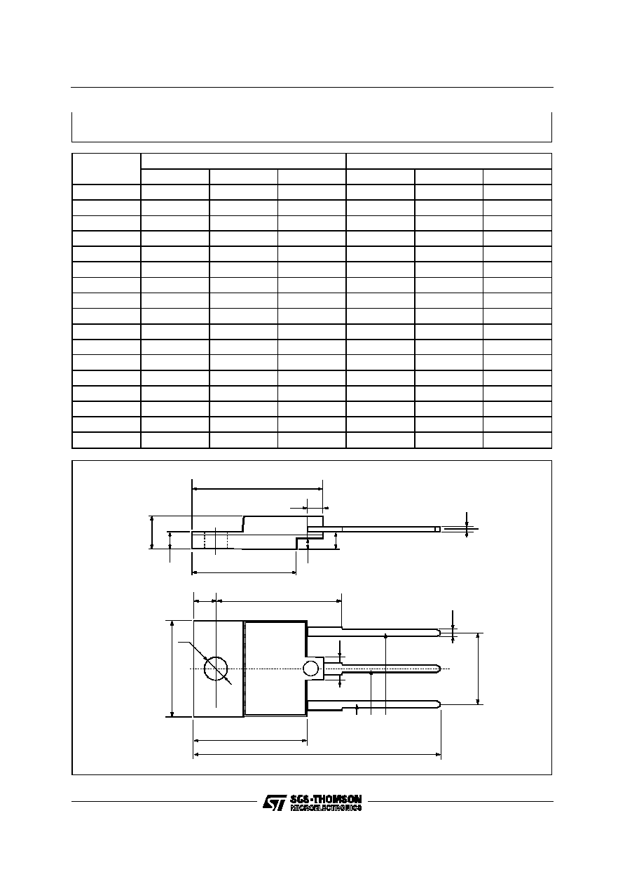
TO-247 MECHANICAL DATA
STW5NA90-STH5NA90FI
4/6
DIM.
mm
inch
MIN.
TYP.
MAX.
MIN.
TYP.
MAX.
A
5.35
5.65
0.210
0.222
C
3.3
3.8
0.130
0.149
D
2.9
3.1
0.114
0.122
D1
1.88
2.08
0.074
0.081
E
0.75
1
0.029
0.039
F
1.05
1.25
0.041
0.049
G
10.8
11.2
0.425
0.441
H
15.8
16.2
0.622
0.637
L1
20.8
21.2
0.818
0.834
L2
19.1
19.9
0.752
0.783
L3
22.8
23.6
0.897
0.929
L4
40.5
42.5
1.594
1.673
L5
4.85
5.25
0.190
0.206
L6
20.25
20.75
0.797
0.817
M
3.5
3.7
0.137
0.145
N
2.1
2.3
0.082
0.090
U
4.6
0.181
L1
A
C
D
E
H
G
M
F
L6
1
2
3
U
L5
L4
D1
N
L3
L2
P025C
ISOWATT218 MECHANICAL DATA
STW5NA90-STH5NA90FI
5/6

Information furnished is believed to be accurate and reliable. However, SGS-THOMSON Microelectronics assumes no responsability for the
consequences of use of such information nor for any infringement of patents or other rights of third parties which may results from its use. No
license is granted by implication or otherwise under any patent or patent rights of SGS-THOMSON Microelectronics. Specifications mentioned
in this publication are subject to change without notice. This publication supersedes and replaces all information previously supplied.
SGS-THOMSON Microelectronics products are not authorized for use as critical components in life support devices or systems without express
written approval of SGS-THOMSON Microelectonics.
©
1998 SGS-THOMSON Microelectronics - Printed in Italy - All Rights Reserved
SGS-THOMSON Microelectronics GROUP OF COMPANIES
Australia - Brazil - Canada - China - France - Germany - Italy - Japan - Korea - Malaysia - Malta - Morocco - The Netherlands -
Singapore - Spain - Sweden - Switzerland - Taiwan - Thailand - United Kingdom - U.S.A
. . .
STW5NA90-STH5NA90FI
6/6