 | ÐлекÑÑоннÑй компоненÑ: STLC30R80 | СкаÑаÑÑ:  PDF PDF  ZIP ZIP |
Äîêóìåíòàöèÿ è îïèñàíèÿ www.docs.chipfind.ru
STLC30R80
INTEGRATED RINGING SLIC
FOR SHORT LOOP APPLICATIONS
MONOCHIP SLIC SUITABLE FOR SHORT
LOOP APPLICATIONS
IMPLEMENTES ALL KEY FEATURES OF
THE BORSHT FUNCTION
INTEGRATED RINGING
SOFT BATTERY REVERSAL WITH PRO-
GRAMMABLE TRANSITION TIME
ON HOOK TRANSMISSION
LOW POWER DISSIPATION IN ALL OPER-
ATING MODES
AUTOMATIC DUAL BATTERY OPERATION
INTEGRATED RING TRIP DETECTION
METERING PULSE INJECTION
LOOP START, GROUND START FEATURES
SURFACE MOUNT PACKAGE
-40 TO +85°C OPERATING RANGE
DESCRIPTION
The STLC30R80 is a SLIC device suitable for
short loop applications. The SLIC provides the
generation of the ringing signal and the standard
battery feeding with full programmability of the DC
characteristic.
In particular two external resistors allow to set the
limiting current value (up to 50mA) and the value
of the resistive feeding when not in constant cur-
rent region.
November 2001
®
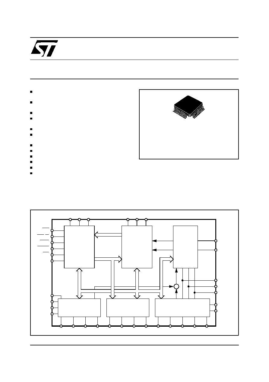
BGND
VREG
ILTF
D0
D1
D2
RS
ZAC
IREF
V
CC
RING
D99TL431AMOD
DET
GDK/AL
CSIN
CAC
AGND CREV CSVR
LOGIC
INTERFACE
&
DECODER
SUPERVISION
COMMANDS
LINE STATUS
ILT
LINE
INTERFACE
ILL
TIP
RT1 RT2
CRT
REFERENCE
&
BIAS SWITCHING
DC
PROCESSOR
+
AC+
DC
AC
DC
RLIM
RTH
ZB
TX
V
DD
VBAT BASE
RDC
AC
PROCESSOR
RX
ZAC1
CSOUT
TTXIN
RES
SW
BLOCK DIAGRAM
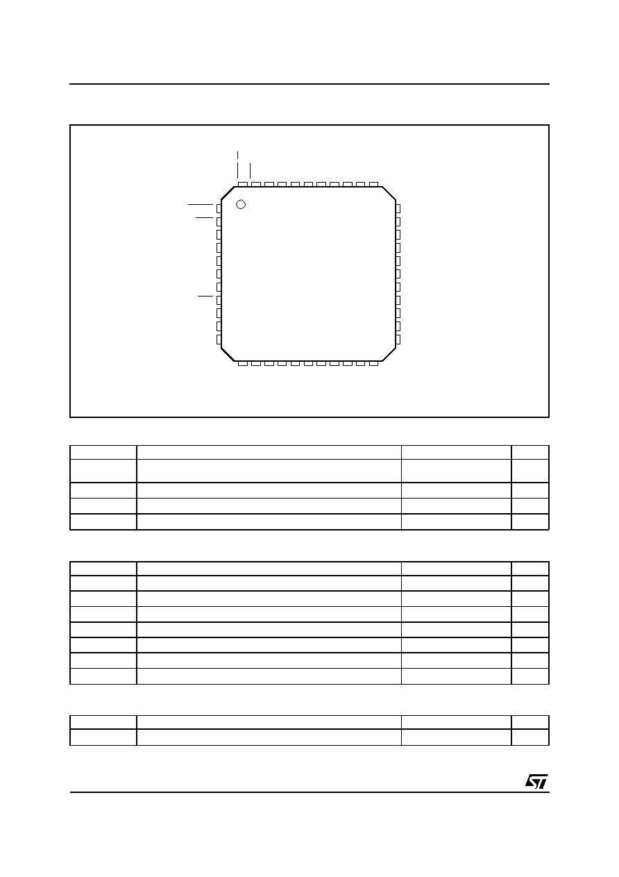
TQFP44 (10 x 10)
ORDERING NUMBER: STLC30R80
1/13
CSOUT
N.C.
CSVR
TTXIN
PINCON_STLC30R80
1
2
3
5
6
4
7
8
9
10
17
11
18 19 20 21 22
44 43 42 41
39
40
38 37 36 35 34
28
27
26
24
23
25
33
32
31
29
30
12 13 14 15 16
CSIN
D0
D1
D2
N.C.
N.C.
RES
VDD
VCC
CRT
N.C.
SW.
AGND
VBAT
TX
ZB
RS
ZAC
ZAC1
RX
CAC
RDC
ILTF
RT2
RT1
AGND
RTH
RLIM
IREF
CREV
BASE
VREG
BGND
RING
TIP
AGND
AGND
AGND
DET
GDK/AL
PIN CONNECTION
ABSOLUTE MAXIMUM RATINGS
Symbol
Parameter
Value
Unit
V
BAT
Battery voltage
-80 + V
CC
to +0.4
-80 + V
REL
to + 0.4
V
V
V
CC
Positive supply voltage
-0.4 to +7
V
V
DD
Control Interface Supply Voltage
-0.4 to +7
V
A/R/BGND
AGND respect BGND
-2 to +2
V
OPERATING RANGE
Symbol
Parameter
Value
Unit
T
opT
Operating temperature range
-40 to +85
°C
V
CC
Positive supply voltage
4.75 to 5.25
V
V
DD
Control Interface Supply Voltage
3 to 5.25
V
V
BAT
Battery voltage
-72 to -15
V
A/BGND
AGND respect BGND
-0.3 to +0.3
V
PD (70)
Max. power dissipation @ Tamb = 70°C
1.1
W
PD(85)
Max. power dissipation @ Tamb = 85°C
0.9
W
THERMAL DATA
Symbol
Parameter
Value
Unit
R
th j-amb
Thermal resistance Junction to Ambient Typ.
60
°C/W
STLC30R80
2/13
PIN DESCRIPTION
Pins
Name
Description
1
CSOUT
Chip-Select for output control bits DET and GDK . Active Low. (*)
2
CSIN
Chip-Select for input control bits latches D0 D1 D2 R0 R1 . Active Low. (*)
3
D0
Control Interface input bit 0. (*)
4
D1
Control Interface input bit 1. (*)
5
D2
Control Interface input bit 2. (*)
6
N.C.
Not connected
7
N.C.
Not connected
8
RES
Reset Input; active low. After activation the SLIC is put in Power Down state
9
V
DD
Control interface Power Supply. V
DD
= 3.3V or V
DD
= V
CC
.
10
V
CC
Positive Power Supply (+5V).
11
CRT
Ring-Trip time constant capacitor.
12
N.C.
Not connected
13
N.C.
Not connected
14
SW
Internal switch/limiting current programming pin.
15
AGND
Analog Ground
16
V
BAT
Negative Battery Supply.
17
TX
4 wires output stage (Transmitting Port).
18
ZB
Cancelling input of Balance Network for 2 to 4 wires conversion.
19
RS
Protection resistors image. The image resistor is connected between this node and ZAC.
20
ZAC
AC impedance synthesis.
21
ZAC1
RX buffer output/ AC impedance is connected between this node and ZAC.
22
RX
4 wires input stage (Receiving Port). A 100K external resistor must be connected to AGND to
bias the input stage.
23
TTXIN
Metering Signal Input (AC) and Line Voltage Drop Programming (DC). If not used must be connectd
to AGND.
24
CAC
AC feedback input/ AC-DC split capacitor is connected between this node and ILTF.
25
RDC
DC current feedback input. The RDC resistor is connected between this node and ILTF.
26
ILTF
Transversal Line Current Image.
27
RT2
Input pin to sense ringing current , for Ring-Trip detection.
28
RT1
Input pin to sense ringing current , for Ring-Trip detection.
29
AGND
Analog ground.
30
RTH
Off-Hook threshold programming pin.
31
RLIM
Limiting current programming pin.
32
IREF
Voltage reference output to generate internal reference current.
33
CREV
Reverse polarity transition time programming.
34
CSVR
Battery supply filter capacitor.
35
BASE
Driver of the external transistor. Connected to the base.
36
VREG
Regulated voltage. Provides the negative supply to the power line drivers. It is connected to the
emitter of the external transistor.
37
BGND
Battery ground.
38
RING
B wire termination output. IB is the current sunk into this pin.
39
TIP
A wire termination output. IA is the current sourced from this pin.
40
AGND
Analog ground.
STLC30R80
3/13
A parallel interface allow to control the operation
of STLC30R80 through a control bus:
- D0 D1 D2 latched input bits defining the Slic
operation mode
- DET and GDK/AL , tri-state outputs, signal the
status of the loop: On/Off-Hook and Ground-Key.
Pin GDK/AL goes low also when the device
thermal protection is activated or a line fault (Tip to
Ring, Tip and/or Ring to Ground or VBAT) is
detected (flowing current
7.5mA).
-CSIN: chip select for input bits, active Low,
strobes the data present on the control bus into
the internal latch.
- CSOUT: chip select for output bits ; active Low ,
when high DET and GDK/AL goes tri-state.
D0 D1 D2 CSIN and CSOUT inputs are provided
with a 15
µ
A pull-down current to prevent uncon-
trolled conditions in case the control bus goes
floating.
According to the table 6 operating modes can be
set:
1) Power-Down.
2) Stand-By.
3) Active N.P.
4) Active R.P.
5) Ringing
6) High Impedance Feeding.
Power-Down
It's an idle state characterised by a very low
power consumption; any functionality is disabled.
It can be set during out of service periods just to
reduce the power consumption.
It is worth noticing that two other conditions can
set the Slic in idle state but with some differences
as reported in the table:
Idle State
DET
GDK/AL
Power Down
Disable
Disable
Reset
Disable
Disable
Thermal Alarm
Low
Low
Stand-By.
Mode selected in On-Hook condition when high
immunity to common mode currents is needed for
the DET bit.
To reduce the current consumption, AC feedback
loop is disabled and only DET and GDK/AL de-
tectors are active.
DC current is limited at 16mA (not programma-
ble); feeding characteristic shown in fig. a.
The voltage drop in on-hook condition is 7.8V.
Active
Mode selected to allow voice signal transmission.
When in ACTIVE mode the voltage drop in on-
hook condition is 7.8V in order to allow proper on-
hook transmission (Fig. b).
Resistive Region is programmable by means of
external resistor R
DC
, limiting current can be se-
lected by R
LIM
and R
switch
resistor.
CONTROL INTERFACE
INPUTS
OPERATING MODE
OUTPUTS
D0
D1
D2
DET
(Active Low)
GDK/AL
(Active Low)
0
0
0
0
1
1
1
0
0
1
1
0
1
1
0
1
0
1
0/1
1
0
Power down
Stand-by
Active N.P.
Active R.P.
Ringing
High Impedance Feeding
Ground Start
disable
off/hk
off/hk
off/hk
ring/trip
off/hk
off/hk
disable
gnd-key
gnd-key
gnd-key
disable
disable
gnd-key
16mA
R
FEED
= 2R
P
D98TL307
V
BAT
-7.8V
I
V
Figure a: STLC30R80 DC Characteristic in
Stand-By Mode.
I
LIM
[20
÷
50mA]
R
FEED
=
R
DC
5
+2R
P
D99TL435
R
FEED
= 2R
P
V
BAT
V
BAT
-7.8V
I
V
Figure b. STLC30R80 DC Characteristic in
Active Mode.
STLC30R80
4/13
Concerning AC characteristic the STLC30R80 al-
lows to set 2W termination impedance by means of
one external scaled impedance that may be com-
plex. Two to four wire conversion is provided by an
external network. Such network can be avoided in
case of application with COMBOII, in this case the
two to four wire conversion is implemented inside
the COMBOII by means of the programmable Hy-
bal filter.
When in ACTIVE mode it is also possible to per-
form battery reversal in soft mode (with program-
mable transition time) without affecting the AC sig-
nal transmission.
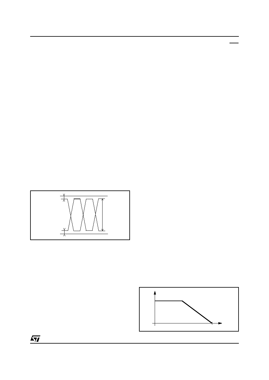
Ringing
When ringing mode is selected, by toggling the
D2 pin is possible to insert the ringing signal on
the line: the ringing frequency is equal to the one
applied to the D2 pin. The ringing signal is a bal-
anced trapezoidal wave form where the TIP and
RING voltages switch continuously between GND
and VREG: VREG is obtained directly from VB1
(VREG = VB1 - 1.8V). The slope of the trapezoi-
dal wave form is set by the external Crev capaci-
tor and it allows to obtain ringing signal with dis-
tortion less than 10%: with a fine tuning of this
capacitor is possible to obtain distortion value
less than 5% (crest factor from 1.25 to 1.35).
The VB1 value must be higher enough (~70V) in
order to obtain ringing signals with more than
40Vrms. The VB2 battery is used only when the
line is in off hook and its value can be reduced
(typ. 24V) in order to minimize the power con-
sumption.
The ring trip detection is performed sensing the
variation of the AC line impedance from on-hook
(relatively high) to off-hook (relatively low). This
particularly ring trip method allows to operate
without DC off-set superimposed on the ringing
signal and therefore obtaining the maximum pos-
sible ring level on the load starting from a given
negative battery.
It should be noted that such a meted is optimized
for operation on short loop applications and may
not operate properly in presence of long loop
(>500 Ohm).
As the ring trip is detected the logic indicator DET
is set low and the ringing is automatically discon-
nected without waiting for the card controller com-
mand (auto ring trip).
Ringing with high REN number
When ringing high number of REN, for example
5REN, or short loops, it could happen that the line
AC current, trigger the ring trip circuit producing
false ring trip.
If this happens, a proper SW resistor (Rswitch)
can be inserted between RLIM and the pin.
The effect of this resistor is to improve the AC
current capability in Ring mode avoiding false ring
trip in presence of high REN numbers (typ.
5REN) and short loop.
One side effect of Rswitch is to reduce ring trip
sensitivity in presence of long loops; therefore it is
recommended to adjust Rswitch properly check-
ing the correct behaviour of the device in the two
worst-case conditions:
- 0
loop, Max REN#
- Max loop length, 1 REN
The lower is the Rswitch value; the higher is the
immunity to false Ring trip, producing as side ef-
fect a lower Ring trip sensitivity on long loops.
The typical value of Rswitch is shown in the Ex-
ternal Components Table (pag.7.13)
High Impedance Feeding.
As Stand-By, this mode is set in On-Hook condi-
tion, with further reduced power consumption.
Higher power efficiency turns back a lower immu-
nity of the Off-Hook detector to line common
mode currents. The DC feeding shows a constant
current characteristic (I
lim
= 17mA) followed by a
resistive range with an equivalent series resis-
tance R
FEED
= 1600
+ 2Rp.
Thermal protection circuit is still active, preventing
the junction temperature, in case of fault condi-
tion, to exceed 150°C
In High Impedance Feeding most of the circuit is
switched off, only the circuit, dedicated to Off-
Hook detection, is powered. This allows to reduce
17mA
R
FEED
= 1600
+2R
P
D98TL373
V
BAT
-0.8V
I
V
Figure d. STLC30R80 DC Characteristic in
High Impedance Feeding
GND
TIP
RING
dV/dT set
by CREV
3V typ.
60V
typ.
VREG
3V typ.
Figure c. Typical ringing wave form.
STLC30R80
5/13