1/8
May 2003
s
RECEIVER AND DRIVERS MEET OR
EXCEED THE REQUIREMENTS OF ANSI
EIA/TIA-644 STANDARD, RECEIVERS
DIFFERENTIAL INPUT LEVELS, ±100mV
s
DESIGNED FOR SIGNALING RATES UP TO
630Mbps
s
OPERATES FROM A SINGLE 3.3V SUPPLY
s
LOW VOLTAGE DIFFERENTIAL SIGNALING
WITH TYPICAL OUTPUT VOLTAGE OF
350mV AND A 100
LOAD
s
PROPAGATION DELAY TIME: 3.1ns (TYP)
s
ELECTRICALLY COMPATIBLE WITH LVDS,
PECL, LVPECL, LVTTL, LVCOMOS, GTL,
BTL, CTT, SSTL, OR HSTL OUTPUTS WITH
EXTERNAL NETWORK
s
BUS TERMINAL ESD (HBM) EXCEEDS 7KV
s
SO AND TSSOP PACKAGING
DESCRIPTION
The STLVDS104 is a differential line receiver and
a LVTTL input connected to four differential line
drivers
that
implement
the
electrical
characteristics of low voltage differential signaling,
for point to point baseband data transmission over
controlled impedance media of approximately
100
.
The
transmission
media
can
be
printed-circuit board traces, backplanes, or cable.
LVDS, as specified in EIA/TIA-644 is a data
signaling technique that offers low-power, low
noise coupling, and switching speed to transmit
data at a speed up to 630Mbps at relatively long
distances.
The drivers integrated into the same substrate,
along with the low pulse skew of balanced
signaling,
allow
extremely
precise
timing
alignment of the signals repeated from the input.
The device allows extremely precise timing
alignment of the signal repeated from the input.
This is particularly advantageous in distribution or
expansion of signals such as clock or serial data
stream.
ORDERING CODES
Type
Temperature
Range
Package
Comments
STLVDS104BD
-40 to 85 ∞C
SO-16 (Tube)
50parts per tube / 20tube per box
STLVDS104BDR
-40 to 85 ∞C
SO-16 (Tape & Reel)
2500 parts per reel
STLVDS104BTR
-40 to 85 ∞C
TSSOP16 (Tape & Reel)
2500 parts per reel
STLVDS104
4-PORT LVDS AND 4-PORT TTL-TO LVDS
REPEATERS
SOP
TSSOP
STLVDS104
2/8
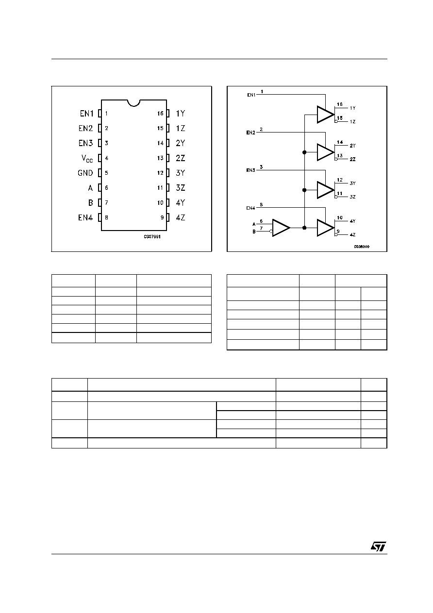
PIN CONFIGURATION
PIN DESCRIPTION
FUNCTIONAL DIAGRAM
FUNCTIONAL TABLE
L=Low level, H=High Level, ?=Indeterminate, Z= High Impedance
ABSOLUTE MAXIMUM RATINGS
Absolute Maximum Ratings are those values beyond which damage to the device may occur. Functional operation under these condition is
not implied.
Note 1: All voltages except differential I/O bus voltage, are with respect to the network ground terminal.
PlN N∞
SYMBOL
NAME AND FUNCTION
1, 2, 3, 8
EN1 to EN4 Enable Driver Inputs
6, 7
A, B
Receiver Input
9, 11, 13, 15
1Z to 4Z
Driver Inputs
10, 12, 14, 16
1X to 4X
Driver Inputs
5
GND
Ground
4
V
CC
Supply Voltage
INPUT
ENABLES
OUTPUTS
V
ID
=V
A
-V
B
#EN
#Y
#Z
X
X
Z
Z
X
L
Z
Z
V
ID
100mV
H
H
L
-100mV < V
ID
<
100mV
H
?
?
V
ID
-
100mV
H
L
H
Symbol
Parameter
Value
Unit
V
CC
Supply Voltage (Note 1)
-0.5 to 4
V
V
R
Voltage Range
Enable Inputs
-0.5 to 6
V
A, B, Y or Z
-0.5 to 4
V
ESD
ESD Protection Voltage (HBM)
Y, Z, to GND
7
KV
All Pins
2
KV
T
stg
Storage Temperature Range
-65 to +150
∞C
STLVDS104
3/8
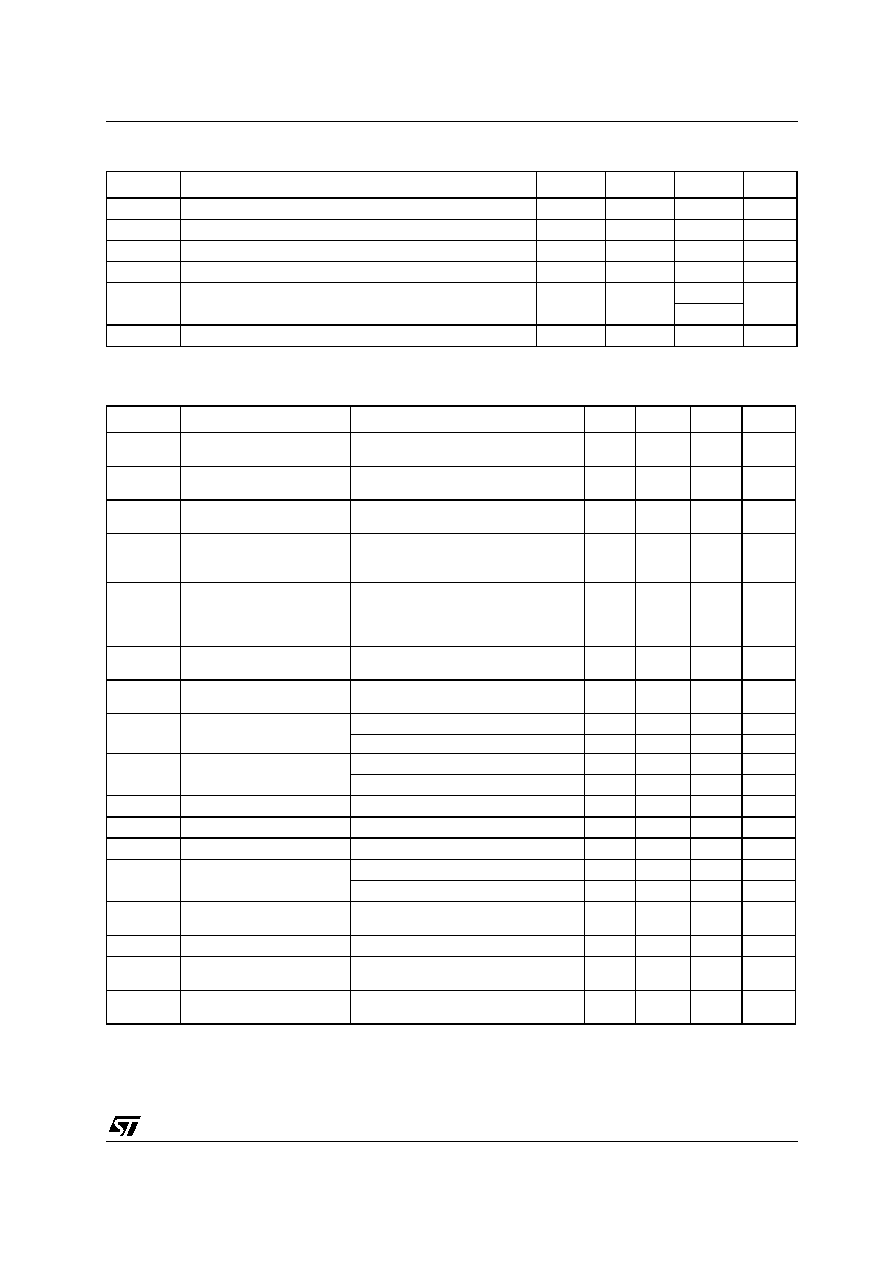
RECOMMENDED OPERATING CONDITIONS
ELECTRICAL CHARACTERISTICS (T
A
= -40 to 85∞C, and V
CC
= 3.3V ±10% over recommended
operating conditions unless otherwise noted. All typical values are at T
A
= 25∞C)
Symbol
Parameter
Min.
Typ.
Max.
Unit
V
CC
Supply Voltage
3.0
3.3
3.6
V
V
IH
HIGH Level Input Voltage
2.0
V
V
IL
LOW Level Input Voltage
0.8
V
|V
ID
|
Magnitude Of Differential Input Voltage
0.1
3.6
V
V
IC
Common Mode Input Voltage
|V
ID
|/2
24-|V
ID
|/2
V
V
CC
-0.8
T
A
Operating Temperature Range
-40
85
∞C
Symbol
Parameter
Test Conditions
Min.
Typ.
Max.
Unit
V
ITH+
Positive-going Differential
Input Voltage Threshold
100
mV
V
ITH-
Negative-going Differential
Input Voltage Threshold
-100
mV
|V
OD
|
Differential Output Voltage
Magnitude
R
L
= 100
V
ID
= ±100mV
247
340
454
mV
|
V
OD
|
Change in Differential
Output Voltage Magnitude
Between Logic State
-50
50
mV
V
OC(SS)
Change in Steady-state
Common Mode Output
Voltage Between Logic
State
-50
50
mV
V
OC(SS)
Steady-state Common
Mode Output Voltage
1.125
1.2
1.375
V
V
OC(PP)
Peak to Paek Common
mode Output Voltage
25
150
mV
I
CC
Supply Current
Enabled, R
L
= 100
20
30
mA
Disabled
2.5
5
mA
I
I
Input Current (A or B
Inputs)
V
I
=0V
-2
-11
-20
µ
A
V
I
= 2.4V
-1
-3
µ
A
I
I(OFF)
Power OFF Input Current
V
CC
= 1.5V
V
I
= 2.4V
3
20
µ
A
I
IH
High Level Input Current
V
IH
= 2V
7
20
µ
A
I
IL
Low Level Input Current
V
IL
= 0.8V
3
10
µ
A
I
OC
Short Circuit Output Current V
O(Y)
or V
O(Z)
= 0V
±
6
±
10
mA
V
OD
= 0
±
3
±
10
mA
I
OZ
High Impedance Output
Current
V
O
= 0 or 2.4V
±
1
µ
A
I
O(OFF)
Power OFF Output Current
V
CC
= 1.5V
V
O
= 2.4V
±
1
µ
A
C
IN
Input Capacitance (A or B
Inputs)
V
I
= 0.4 sin (4e
6
t
)+0.5V
3
pF
C
O
Output Capacitance (Y or Z
Outputs)
V
I
= 0.4 sin (4e
6
t
)+0.5V, Disabled
6
pF
STLVDS104
4/8
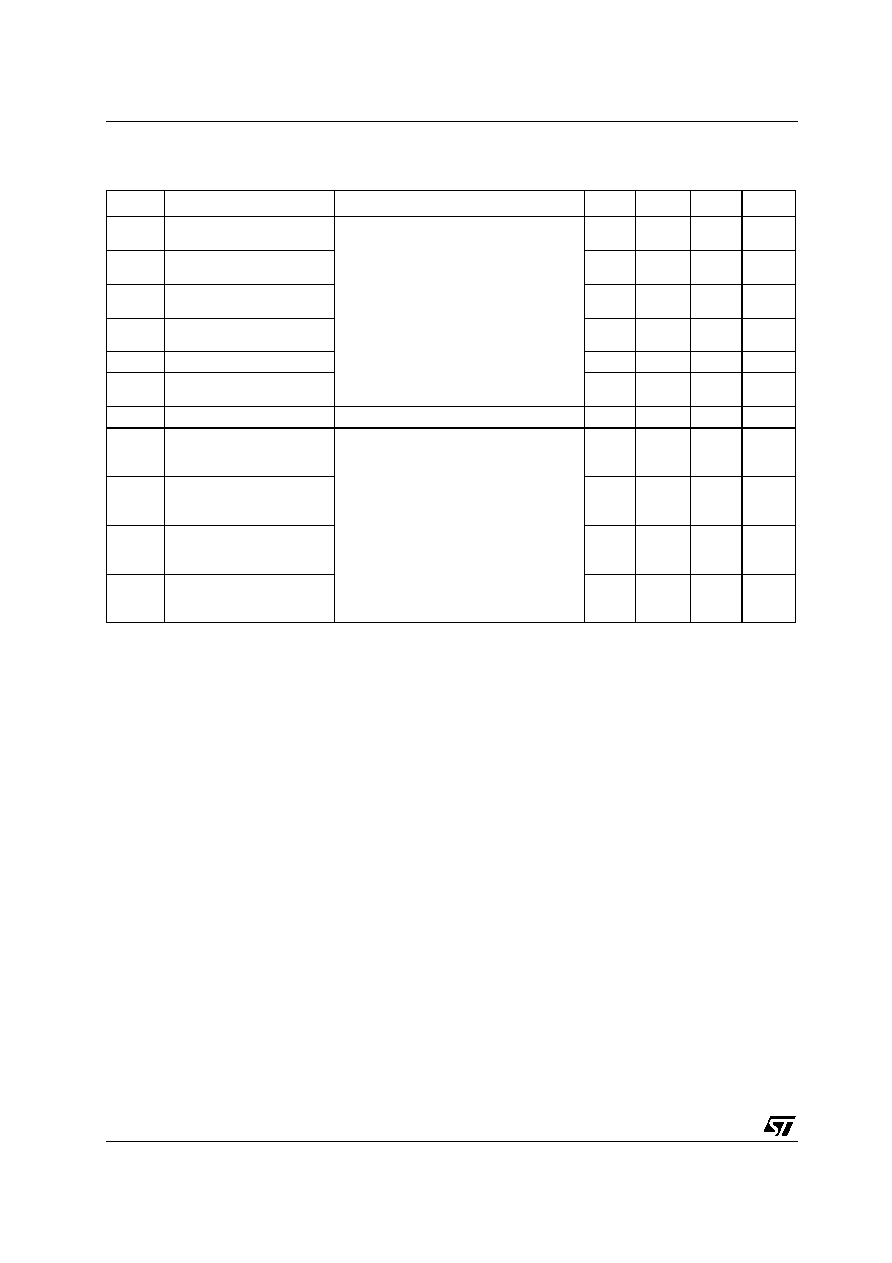
SWITCHING CHARACTERISTICS (T
A
= -40 to 85∞C, and V
CC
= 3.3V unless otherwise noted. All typical
values are at T
A
= 25∞C)
Note 1: t
sk(O)
is the time difference between the t
PLH
or t
PHL
of all drivers of a single device with all their inputs connected together.
Note 2: t
sk(pp)
is the magnitude of the difference in propagation delay times between any specified terminals of two devices when both devices
operate with the same supply voltages, at the same temperature, and have identical packages and test circuit.
Symbol
Parameter
Test Conditions
Min.
Typ.
Max.
Unit
t
PLH
Propagation Delay Time,
Low to High Output
R
L
= 100
C
L
= 10pF
2.4
3.2
4.2
ns
t
PHL
Propagation Delay Time,
High to Low Output
2.2
3.1
4.2
ns
t
r
Differential Output Signal
Rise Time
0.3
0.7
1.2
ns
t
f
Differential Output Signal
Fall Time
0.3
0.7
1.2
ns
t
sk(P)
Pulse Skew (|t
THL
- t
TLH
|)
100
300
ps
t
sk(O)
Channel-to-channel Output
Skew (note1)
50
100
ps
t
sk(pp)
Part to part Skew (note2)
1.5
ns
t
PZH
Propagation Delay Time,
High Impedance to High
Level Output
7.2
15
ns
t
PZL
Propagation Delay Time,
High Impedance to Low
Level Output
8.4
15
ns
t
PHZ
Propagation Delay Time,
High Level to High
Impedance Output
3.6
15
ns
t
PLZ
Propagation Delay Time,
Low Level to High
Impedance Output
6
15
ns
STLVDS104
5/8
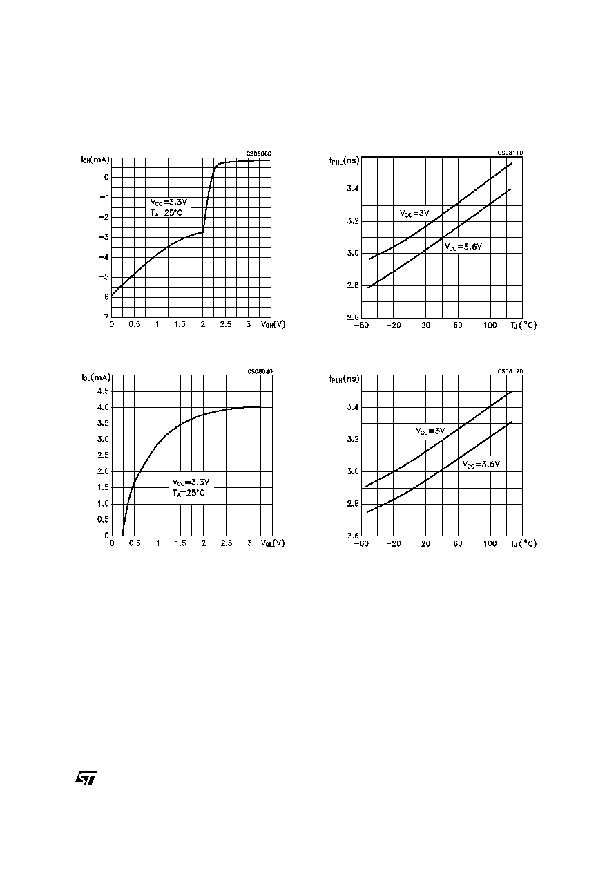
TYPICAL PERFORMANCE CHARACTERISTICS (unless otherwise specified T
j
= 25∞C)
Figure 1 : Output Current vs Output High Voltage
Figure 2 : Output Current vs Output Low Voltage
Figure 3 : High to Low Propagation Delay Time
Figure 4 : Low to High Propagation Delay Time