
1/21
October 2005
STM1061
Low Power Voltage Detector
Rev 2.0
FEATURES
FACTORY-TRIMMED VOLTAGE
THRESHOLDS IN 0.1V INCREMENTS
FROM 1.6V TO 5.5V
±2% VOLTAGE THRESHOLD ACCURACY
OPERATING VOLTAGE 0.7V to 6.0V
OPEN DRAIN OUTPUT
LOW SUPPLY CURRENT - 0.9µA (typ)
GUARANTEED OUT ASSERTION DOWN
TO V
CC
= 0.7V
POWER SUPPLY TRANSIENT IMMUNITY
AVAILABLE IN SOT23-3 and SOT323-3
(SC70-3) PACKAGES
OPERATING TEMPERATURE ≠40∞C TO
85∞C
Figure 1. Packages
Note: 1. Contact local sales office for availability.
SOT323-3, SC70-3 (W)
(1)
SOT23-3 (WX)

STM1061
2/21
TABLE OF CONTENTS
FEATURES . . . . . . . . . . . . . . . . . . . . . . . . . . . . . . . . . . . . . . . . . . . . . . . . . . . . . . . . . . . . . . . . . . . . . . . 1
Figure 1. Packages . . . . . . . . . . . . . . . . . . . . . . . . . . . . . . . . . . . . . . . . . . . . . . . . . . . . . . . . . . . . . . 1
SUMMARY DESCRIPTION . . . . . . . . . . . . . . . . . . . . . . . . . . . . . . . . . . . . . . . . . . . . . . . . . . . . . . . . . . . 4
Figure 2. Logic Diagram . . . . . . . . . . . . . . . . . . . . . . . . . . . . . . . . . . . . . . . . . . . . . . . . . . . . . . . . . . 4
Table 1. Signal Names . . . . . . . . . . . . . . . . . . . . . . . . . . . . . . . . . . . . . . . . . . . . . . . . . . . . . . . . . . 4
Figure 3. SOT23-3 Connections . . . . . . . . . . . . . . . . . . . . . . . . . . . . . . . . . . . . . . . . . . . . . . . . . . . . 4
Figure 4. SOT323-3 (SC70-3) Connections . . . . . . . . . . . . . . . . . . . . . . . . . . . . . . . . . . . . . . . . . . . 4
Figure 5. N-Channel Open Drain Output Block Diagram . . . . . . . . . . . . . . . . . . . . . . . . . . . . . . . . . 5
Figure 6. STM1061N Active-Low, Open Drain Hardware Hookup . . . . . . . . . . . . . . . . . . . . . . . . . . 5
PIN DESCRIPTIONS . . . . . . . . . . . . . . . . . . . . . . . . . . . . . . . . . . . . . . . . . . . . . . . . . . . . . . . . . . . . . . . . 6
Table 2. Pin Functions . . . . . . . . . . . . . . . . . . . . . . . . . . . . . . . . . . . . . . . . . . . . . . . . . . . . . . . . . . . 6
OPERATION . . . . . . . . . . . . . . . . . . . . . . . . . . . . . . . . . . . . . . . . . . . . . . . . . . . . . . . . . . . . . . . . . . . . . . 6
Output. . . . . . . . . . . . . . . . . . . . . . . . . . . . . . . . . . . . . . . . . . . . . . . . . . . . . . . . . . . . . . . . . . . . . . . . 6
Negative-Going V
CC
Transients and Undershoot. . . . . . . . . . . . . . . . . . . . . . . . . . . . . . . . . . . . . 6
TYPICAL OPERATING CHARACTERISTICS . . . . . . . . . . . . . . . . . . . . . . . . . . . . . . . . . . . . . . . . . . . . 7
Figure 7. Supply Current vs. Input Voltage . . . . . . . . . . . . . . . . . . . . . . . . . . . . . . . . . . . . . . . . . . . . 7
Figure 8. Supply Current vs. Ambient Temperature . . . . . . . . . . . . . . . . . . . . . . . . . . . . . . . . . . . . . 7
Figure 9. Output Detect Delay Time vs. Ambient Temperature . . . . . . . . . . . . . . . . . . . . . . . . . . . . 8
Figure 10.Output Release Delay Time vs. Ambient Temperature . . . . . . . . . . . . . . . . . . . . . . . . . . . 8
Figure 11.Maximum Transient Duration vs. Reset Threshold Overdrive. . . . . . . . . . . . . . . . . . . . . . 9
Figure 12.Detect, Release Voltage vs. Ambient Temperature for V
TH≠
= 3.4V. . . . . . . . . . . . . . . . . 9
Figure 13.N-channel Driver Output Current vs. V
DS . . . . . . . . . . . . . . . . . . . . . . . . . . . . . . . . . . . . . . . . . . . . . . 10
Figure 14.N-channel Driver Output Current vs. Input Voltage . . . . . . . . . . . . . . . . . . . . . . . . . . . . . 10
MAXIMUM RATING. . . . . . . . . . . . . . . . . . . . . . . . . . . . . . . . . . . . . . . . . . . . . . . . . . . . . . . . . . . . . . . . 11
Table 3. Absolute Maximum Ratings . . . . . . . . . . . . . . . . . . . . . . . . . . . . . . . . . . . . . . . . . . . . . . . 11
DC AND AC PARAMETERS. . . . . . . . . . . . . . . . . . . . . . . . . . . . . . . . . . . . . . . . . . . . . . . . . . . . . . . . . 12
Table 4. Operating and AC Measurement Conditions . . . . . . . . . . . . . . . . . . . . . . . . . . . . . . . . . . 12
Figure 15.AC Testing Input/Output Waveforms. . . . . . . . . . . . . . . . . . . . . . . . . . . . . . . . . . . . . . . . 12
Figure 16.Voltage Timing Waveform . . . . . . . . . . . . . . . . . . . . . . . . . . . . . . . . . . . . . . . . . . . . . . . . 12
Table 5. DC and AC Characteristics . . . . . . . . . . . . . . . . . . . . . . . . . . . . . . . . . . . . . . . . . . . . . . . 13
PACKAGE MECHANICAL . . . . . . . . . . . . . . . . . . . . . . . . . . . . . . . . . . . . . . . . . . . . . . . . . . . . . . . . . . 14
Figure 17.SOT23-3 ≠ 3-lead Small Outline Transistor Package Outline . . . . . . . . . . . . . . . . . . . . . 15
Table 6. SOT23-3 ≠ 3-lead Small Outline Transistor Package Mechanical Data . . . . . . . . . . . . . 15
Figure 18.SOT323-3 (SC70-3) ≠ 3-lead Small Outline Transistor Package Outline . . . . . . . . . . . . 16
Table 7. SOT323-3 (SC70-3) ≠ 3-lead Small Outline Transistor Package Mechanical Data . . . . 16
STM1061
4/21
SUMMARY DESCRIPTION
The STM1061 low power voltage detector pro-
vides monitoring of battery, power-supply, and
regulated system voltages. A precision voltage
reference and comparator monitors the V
CC
input
and compares it with a specified voltage threshold
condition. When V
CC
falls below a specified trip
point threshold, the output (OUT) is forced low and
remains asserted as long as the V
CC
input re-
mains below V
TH≠
+ hysteresis (V
HYST
). The
STM1061 device is guaranteed to output the cor-
rect logic state for V
CC
down to 0.7V. They are
also designed to ignore fast transients on V
CC
.
This small, low power device is ideal for portable
applications and is available in space-saving
SOT23-3 and SOT323-3 (SC70-3) packages.
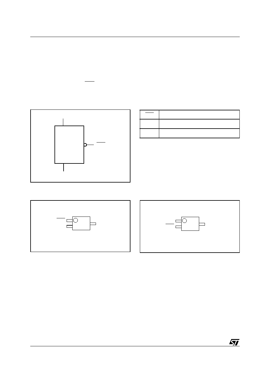
Figure 2. Logic Diagram
Table 1. Signal Names
Figure 3. SOT23-3 Connections
Figure 4. SOT323-3 (SC70-3) Connections
AI10477
V
CC
STM1061
V
SS
OUT
OUT
Open Drain Active-Low Output
V
CC
Supply Voltage
V
SS
Ground
AI10478
2
3
1
OUT
VCC
VSS
AI10479
2
3
1
OUT
VCC
VSS

