 | –≠–ª–µ–∫—Ç—Ä–æ–Ω–Ω—ã–π –∫–æ–º–ø–æ–Ω–µ–Ω—Ç: STN4NE03 | –°–∫–∞—á–∞—Ç—å:  PDF PDF  ZIP ZIP |

STN4NE03
N - CHANNEL 30V - 0.045
- 4A - SOT-223
STripFET
TM
POWER MOSFET
s
TYPICAL R
DS(on)
= 0.045
s
EXCEPTIONAL dv/dt CAPABILITY
s
AVALANCHE RUGGED TECHNOLOGY
s
100% AVALANCHE TESTED
s
APPLICATION ORIENTED
CHARACTERIZATION
DESCRIPTION
This Power MOSFET is the latest development of
STMicroelectronics unique "
Single Feature
Size
TM
"
strip-based process. The resulting
transistor shows extremely high packing density
for
low
on-resistance,
rugged
avalanche
characteristics and less critical alignment steps
therefore
a
remarkable
manufacturing
reproducibility.
APPLICATIONS
s
DC MOTOR CONTROL (DISK DRIVES, etc.)
s
DC-DC & DC-AC CONVERTERS
s
SYNCHRONOUS RECTIFICATION
s
POWER MANAGEMENT IN
BATTERY-OPERATED AND PORTABLE
EQUIPMENT
Æ
INTERNAL SCHEMATIC DIAGRAM
August 1998
1
2
2
3
SOT-223
ABSOLUTE MAXIMUM RATINGS
Symbol
Parameter
Val ue
Uni t
V
DS
Drain-source Voltage (V
GS
= 0)
30
V
V
DGR
Drain- gate Voltage (R
G S
= 20 k
)
30
V
V
GS
Gate-source Voltage
±
20
V
I
D
(*)
Drain Current (cont inuous) at T
c
= 25
o
C
4
A
I
D
(*)
Drain Current (cont inuous) at T
c
= 100
o
C
2.5
A
I
DM
(
∑
)
Drain Current (pulsed)
16
A
P
t ot
Tot al Dissipation at T
c
= 25
o
C
2.5
W
Derating Fact or
0. 02
W/
o
C
dv/dt (
1
)
Peak Diode Recovery voltage slope
6
V/ ns
T
stg
St orage Temperature
-65 to 150
o
C
T
j
Max. Operat ing Junction Temperat ure
150
o
C
(
∑
) Pulse width limited by safe operating area
(*) Limited by package
(1)I
SD
10A, di/dt
300A/
µ
s, V
DD
V
(BR)DSS
, Tj
T
jMAX
TYPE
V
DSS
R
DS(on)
I
D
ST N4NE03
30 V
< 0.06
4 A
1/8

THERMAL DATA
R
thj -pcb
R
t hj- amb
T
l
Thermal Resistance Junction-PC Board
Max
Thermal Resistance Junction-ambient
Max
(Surface Mount ed)
Maximum Lead Temperature For Soldering Purpose
50
60
260
o
C/W
o
C/W
o
C
AVALANCHE CHARACTERISTICS
Symb ol
Parameter
Max Valu e
Uni t
I
AR
Avalanche Current, Repetitive or Not -Repet itive
(pulse width limited by T
j
max,
< 1%)
4
A
E
AS
Single Pulse Avalanche Energy
(starting T
j
= 25
o
C, I
D
= I
AR
, V
DD
= 25 V)
20
mJ
ELECTRICAL CHARACTERISTICS (T
case
= 25
o
C unless otherwise specified)
OFF
Symb ol
Parameter
Test Cond ition s
Mi n.
Typ .
Max.
Un it
V
(BR)DSS
Drain-source
Breakdown Volt age
I
D
= 250
µ
A
V
GS
= 0
30
V
I
DSS
Zero G ate Voltage
Drain Current (V
GS
= 0)
V
DS
= Max Rating
V
DS
= Max Rating
T
c
= 125
o
C
1
10
µ
A
µ
A
I
GSS
Gate-body Leakage
Current (V
DS
= 0)
V
G S
=
±
20 V
±
100
nA
ON (
)
Symb ol
Parameter
Test Cond ition s
Mi n.
Typ .
Max.
Un it
V
GS(th)
Gate Threshold
Voltage
V
DS
= V
GS
I
D
= 250
µ
A
2
3
4
V
R
DS( on)
St atic Drain-source On
Resistance
V
G S
= 10 V
I
D
= 2 A
0.045
0.06
I
D(o n)
On St ate Drain Current
V
DS
> I
D(on)
x R
DS(on) max
V
G S
= 10 V
4
A
DYNAMIC
Symb ol
Parameter
Test Cond ition s
Mi n.
Typ .
Max.
Un it
g
fs
(
)
Forward
Transconduct ance
V
DS
> I
D(on)
x R
DS(on) max
I
D
= 2 A
1
3.0
S
C
iss
C
oss
C
rss
Input Capacitance
Output Capacit ance
Reverse T ransfer
Capacitance
V
DS
= 25 V
f = 1 MHz
V
GS
= 0 V
760
150
50
1000
200
80
pF
pF
pF
Æ
STN4NE03
2/8

ELECTRICAL CHARACTERISTICS (continued)
SWITCHING ON
Symb ol
Parameter
Test Cond ition s
Mi n.
Typ .
Max.
Un it
t
d(on)
t
r
Turn-on Time
Rise Time
V
DD
= 5 V
I
D
= 5 A
R
G
= 4.7
V
G S
= 10 V
(see test circuit, figure 3)
10
60
15
90
ns
ns
Q
g
Q
gs
Q
gd
Total Gate Charge
Gate-Source Charge
Gate-Drain Charge
V
DD
= 24 V
I
D
= 10 A
V
GS
= 10 V
22
7
7
30
nC
nC
nC
SWITCHING OFF
Symb ol
Parameter
Test Cond ition s
Mi n.
Typ .
Max.
Un it
t
r(Vof f)
t
f
t
c
Of f-voltage Rise Time
Fall Time
Cross-over Time
V
DD
= 24 V
I
D
= 10 A
R
G
= 4.7
V
GS
= 10 V
(see test circuit, figure 5)
8
15
25
15
25
40
ns
ns
ns
SOURCE DRAIN DIODE
Symb ol
Parameter
Test Cond ition s
Mi n.
Typ .
Max.
Un it
I
SD
I
SDM
(
∑
)
Source-drain Current
Source-drain Current
(pulsed)
4
16
A
A
V
SD
(
)
Forward On Voltage
I
SD
= 4 A
V
GS
= 0
1.5
V
t
rr
Q
rr
I
RRM
Reverse Recovery
Time
Reverse Recovery
Charge
Reverse Recovery
Current
I
SD
= 10 A
di/dt = 100 A/
µ
s
V
DD
= 24 V
T
j
= 150
o
C
(see test circuit, figure 5)
40
0. 06
3.0
ns
µ
C
A
(
) Pulsed: Pulse duration = 300
µ
s, duty cycle 1.5 %
(
∑
) Pulse width limited by safe operating area
Safe Operating Area
Thermal Impedance
Æ
STN4NE03
3/8

Output Characteristics
Transconductance
Gate Charge vs Gate-source Voltage
Transfer Characteristics
Static Drain-source On Resistance
Capacitance Variations
Æ
STN4NE03
4/8
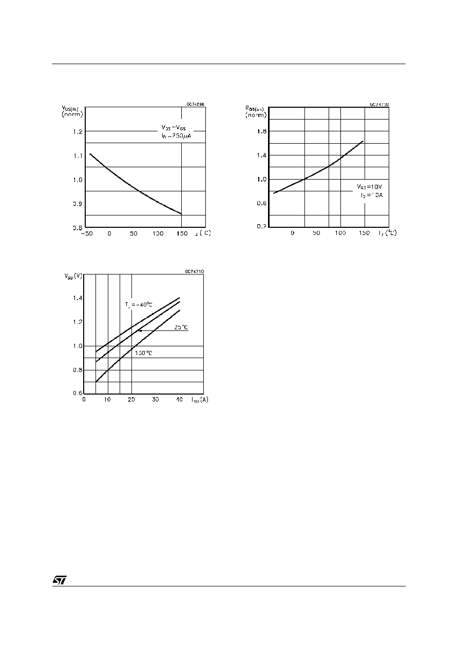
Normalized Gate Threshold Voltage vs
Temperature
Source-drain Diode Forward Characteristics
Normalized On Resistance vs Temperature
Æ
STN4NE03
5/8