 | –≠–ª–µ–∫—Ç—Ä–æ–Ω–Ω—ã–π –∫–æ–º–ø–æ–Ω–µ–Ω—Ç: STN851 | –°–∫–∞—á–∞—Ç—å:  PDF PDF  ZIP ZIP |

STN851
LOW VOLTAGE FAST-SWITCHING
NPN POWER TRANSISTOR
PRELIMINARY DATA
s
VERY LOW COLLECTOR TO EMITTER
SATURATION VOLTAGE
s
HIGH CURRENT GAIN CHARACTERISTIC
s
FAST-SWITCHING SPEED
s
SURFACE-MOUNTING SOT-223 MEDIUM
POWER PACKAGE IN TAPE & REEL
APPLICATIONS:
s
EMERGENCY LIGHTING
s
VOLTAGE REGULATORS
s
RELAY DRIVERS
s
HIGH EFFICIENCY LOW VOLTAGE
SWITCHING APPLICATIONS
DESCRIPTION
The device is manufactured in NPN Planar
Technology by using a "Base Island" layout.
The resulting Transistor shows exceptional high
gain performance coupled with very low
saturation voltage.
Æ
INTERNAL SCHEMATIC DIAGRAM
September 2003
ABSOLUTE MAXIMUM RATINGS
Symbol
Parameter
Value
Unit
V
CBO
Collector-Base Voltage (I
E
= 0)
150
V
V
CEO
Collector-Emitter Voltage (I
B
= 0)
60
V
V
EBO
Emitter-Base Voltage (I
C
= 0)
7
V
I
C
Collector Current
5
A
I
CM
Collector Peak Current (t
p
< 5 ms)
10
A
I
B
Base Current
1
A
I
BM
Base Peak Current (t
p
< 5 ms)
2
A
P
tot
Total Dissipation at T
amb
= 25
o
C
1.6
W
T
stg
Storage Temperature
-65 to 150
o
C
T
j
Max. Operating Junction Temperature
150
o
C
1
2
2
3
SOT-223
Ordering Code
Marking
Shipment
STN851
N851
Tape & Reel
1/7

THERMAL DATA
R
thj-amb
Thermal Resistance Junction-ambient Max
78
o
C/W
∑
Device mounted on a P.C.B. area of 1 cm
2
ELECTRICAL CHARACTERISTICS (T
case
= 25
o
C unless otherwise specified)
Symbol
Parameter
Test Conditions
Min.
Typ.
Max.
Unit
I
CBO
Collector Cut-off
Current (I
E
= 0)
V
CB
= 120 V
V
CB
= 120 V T
j
= 100
o
C
50
1
nA
µ
A
I
EBO
Emitter Cut-off Current
(I
C
= 0)
V
EB
= 7 V
10
nA
V
(BR)CBO
Collector-Base
Breakdown Voltage
(I
E
= 0)
I
C
= 100
µ
A
150
V
V
(BR)CEO
Collector-Emitter
Breakdown Voltage
(I
B
= 0)
I
C
= 10 mA
60
V
V
(BR)EBO
Emitter-Base
Breakdown Voltage
(I
C
= 0)
I
E
= 100
µ
A
7
V
V
CE(sat)
Collector-Emitter
Saturation Voltage
I
C
= 100 mA I
B
= 5 mA
I
C
= 1 A I
B
= 50 mA
I
C
= 2 A I
B
= 50 mA
I
C
= 5 A I
B
= 200 mA
10
70
140
320
50
120
250
500
mV
mV
mV
mV
V
BE(sat)
Base-Emitter
Saturation Voltage
I
C
= 4 A I
B
= 200 mA
1
1.15
V
V
BE(on)
Base-Emitter On
Voltage
I
C
= 4 A V
CE
= 1 V
0.89
1
V
h
FE
DC Current Gain
I
C
= 10 mA V
CE
= 1 V
I
C
= 2 A V
CE
= 1 V
I
C
= 5 A V
CE
= 1 V
I
C
= 10 A V
CE
= 1 V
150
150
90
30
300
270
140
50
350
f
T
Transition frequency
V
CE
= 10 V I
C
= 100 mA
130
MHz
C
CBO
Collector-Base
Capacitance
V
CB
= 10 V f = 1 MHz
50
pF
t
on
t
s
t
f
RESISTIVE LOAD
Turn- on Time
Storage Time
Fall Time
I
C
= 1 A V
CC
= 10 V
I
B1
= - I
B2
= 0.1 A
50
1.35
120
ns
µ
s
ns
* Pulsed: Pulse duration = 300
µ
s, duty cycle = 1.5 %
STN851
2/7

Base-Emitter Saturation Voltage
Base-Emitter On Voltage
Collector-Emitter Saturation Voltage
Collector-Emitter Saturation Voltage
Derating Curve
DC Current Gain
STN851
3/7

Switching Times Inductive Load
Switching Times Resistive Load
Switching Times Inductive Load
Switching Times Resistive Load
Switching Times Resistive Load
STN851
4/7
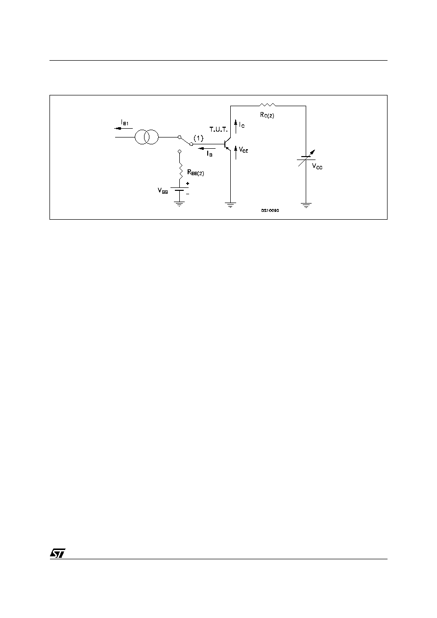
Figure 1: Resistive Load Switching Test Circuit.
1) Fast electronic switch
2) Non-inductive Resistor
STN851
5/7