 | –≠–ª–µ–∫—Ç—Ä–æ–Ω–Ω—ã–π –∫–æ–º–ø–æ–Ω–µ–Ω—Ç: STP11NM60 | –°–∫–∞—á–∞—Ç—å:  PDF PDF  ZIP ZIP |
1/12
May 2003
STP11NM60 - STP11NM60FP
STB11NM60 - STB11NM60-1
N-CHANNEL 600V - 0.4
-11A TO-220/TO-220FP/D
2
PAK/I
2
PAK
MDmeshTMPower MOSFET
(*)Limited only by maximum temperature allowed
(1)I
SD
<11A, di/dt<400A/µs, V
DD
<V
(BR)DSS
, T
J
<T
JMAX
TYPICAL R
DS
(on) = 0.4
HIGH dv/dt AND AVALANCHE CAPABILITIES
100% AVALANCHE TESTED
LOW INPUT CAPACITANCE AND GATE
CHARGE
LOW GATE INPUT RESISTANCE
DESCRIPTION
The MDmeshTM is a new revolutionary MOSFET
technology that associates the Multiple Drain pro-
cess with the Company's PowerMESHTM horizontal
layout. The resulting product has an outstanding low
on-resistance, impressively high dv/dt and excellent
avalanche characteristics. The adoption of the
Company's proprietary strip technique yields overall
dynamic performance that is significantly better than
that of similar competition's products.
APPLICATIONS
The MDmeshTM family is very suitable for increasing
power density of high voltage converters allowing
system miniaturization and higher efficiencies.
ABSOLUTE MAXIMUM RATINGS
(∑)Pulse width limited by safe operating area
TYPE
V
DSS
R
DS(on)
I
D
STP11NM60
STP11NM60FP
STB11NM60
STB11NM60-1
600 V
600 V
600 V
600 V
< 0.45
< 0.45
< 0.45
< 0.45
11 A
11 A
11 A
11 A
Symbol
Parameter
Value
Unit
STP(B)11NM60(-1)
STP11NM60FP
V
DS
Drain-source Voltage (V
GS
= 0)
600
V
V
DGR
Drain-gate Voltage (R
GS
= 20 k
)
600
V
V
GS
Gate- source Voltage
±30
V
I
D
Drain Current (continuous) at T
C
= 25∞C
11
11 (*)
A
I
D
Drain Current (continuous) at T
C
= 100∞C
7
7 (*)
A
I
DM
( )
Drain Current (pulsed)
44
44 (*)
A
P
TOT
Total Dissipation at T
C
= 25∞C
160
35
W
Derating Factor
1.28
0.28
W/∞C
dv/dt(1)
Peak Diode Recovery voltage slope
15
V/ns
V
ISO
Insulation Winthstand Voltage (DC)
--
2500
V
T
stg
Storage Temperature
≠65 to 150
∞C
T
j
Max. Operating Junction Temperature
150
∞C
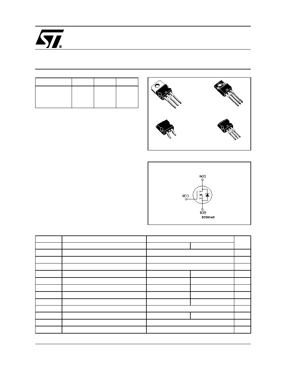
TO-220
1
2
3
1
2
3
I
2
PAK
1
2
3
TO-220FP
1
3
D
2
PAK
INTERNAL SCHEMATIC DIAGRAM

STP11NM60 / STP11NM60FP / STB11NM60 / STB11NM60-1
2/12
THERMAL DATA
AVALANCHE CHARACTERISTICS
ELECTRICAL CHARACTERISTICS (T
CASE
= 25 ∞C UNLESS OTHERWISE SPECIFIED)
OFF
ON (1)
DYNAMIC
1. Pulsed: Pulse duration = 300 µs, duty cycle 1.5 %.
2. C
oss eq.
is defined as a constant equivalent capacitance giving the same charging time as C
oss
when V
DS
increases from 0 to 80%
V
DSS
.
TO-220/D
2
PAK/I
2
PAK
TO-220FP
Rthj-case
Thermal Resistance Junction-case
Max
0.78
3.57
∞C/W
Rthj-amb
Thermal Resistance Junction-ambient
Max
62.5
∞C/W
T
l
Maximum Lead Temperature For Soldering Purpose
300
∞C
Symbol
Parameter
Max Value
Unit
I
AR
Avalanche Current, Repetitive or Not-Repetitive
(pulse width limited by T
j
max)
5.5
A
E
AS
Single Pulse Avalanche Energy
(starting T
j
= 25 ∞C, I
D
= I
AR
, V
DD
= 50 V)
350
mJ
Symbol
Parameter
Test Conditions
Min.
Typ.
Max.
Unit
V
(BR)DSS
Drain-source
Breakdown Voltage
I
D
= 250 µA, V
GS
= 0
600
V
I
DSS
Zero Gate Voltage
Drain Current (V
GS
= 0)
V
DS
= Max Rating
1
µA
V
DS
= Max Rating, T
C
= 125 ∞C
10
µA
I
GSS
Gate-body Leakage
Current (V
DS
= 0)
V
GS
= ±30V
±100
nA
Symbol
Parameter
Test Conditions
Min.
Typ.
Max.
Unit
V
GS(th)
Gate Threshold Voltage
V
DS
= V
GS
, I
D
= 250µA
3
4
5
V
R
DS(on)
Static Drain-source On
Resistance
V
GS
= 10V, I
D
= 5.5A
0.4
0.45
Symbol
Parameter
Test Conditions
Min.
Typ.
Max.
Unit
g
fs
(1)
Forward Transconductance
V
DS
> I
D(on)
x R
DS(on)max,
I
D
= 5.5A
5.2
S
C
iss
Input Capacitance
V
DS
= 25V, f = 1 MHz, V
GS
= 0
1000
pF
C
oss
Output Capacitance
230
pF
C
rss
Reverse Transfer
Capacitance
25
pF
C
oss eq.
(2)
Equivalent Output
Capacitance
V
GS
= 0V, V
DS
= 0V to 480V
100
pF
R
G
Gate Input Resistance
f=1 MHz Gate DC Bias = 0
Test Signal Level = 20mV
Open Drain
1.6

3/12
STP11NM60 / STP11NM60FP / STB11NM60 / STB11NM60-1
ELECTRICAL CHARACTERISTICS (CONTINUED)
SWITCHING ON
SWITCHING OFF
SOURCE DRAIN DIODE
Note: 1. Pulsed: Pulse duration = 300 µs, duty cycle 1.5 %.
2. Pulse width limited by safe operating area.
Symbol
Parameter
Test Conditions
Min.
Typ.
Max.
Unit
t
d(on)
Turn-on Delay Time
V
DD
= 300V, I
D
= 5.5A
R
G
= 4.7
V
GS
= 10V
(see test circuit, Figure 3)
20
ns
t
r
Rise Time
20
ns
Q
g
Total Gate Charge
V
DD
= 400V, I
D
= 11A,
V
GS
= 10V
30
nC
Q
gs
Gate-Source Charge
10
nC
Q
gd
Gate-Drain Charge
15
nC
Symbol
Parameter
Test Conditions
Min.
Typ.
Max.
Unit
t
r(Voff)
Off-voltage Rise Time
V
DD
= 400V, I
D
= 11A,
R
G
= 4.7
,
V
GS
= 10V
(see test circuit, Figure 5)
6
ns
t
f
Fall Time
11
ns
t
c
Cross-over Time
19
ns
Symbol
Parameter
Test Conditions
Min.
Typ.
Max.
Unit
I
SD
Source-drain Current
11
A
I
SDM
(2)
Source-drain Current (pulsed)
44
A
V
SD
(1)
Forward On Voltage
I
SD
= 11A, V
GS
= 0
1.5
V
t
rr
Q
rr
I
rrm
Reverse Recovery Time
Reverse Recovery Charge
Reverse Recovery Current
I
SD
= 11A, di/dt = 100A/µs,
V
DD
= 100 V, T
j
= 25∞C
(see test circuit, Figure 5)
390
3.8
19.5
ns
µC
A
t
rr
Q
rr
I
rrm
Reverse Recovery Time
Reverse Recovery Charge
Reverse Recovery Current
I
SD
= 11A, di/dt = 100A/µs,
V
DD
= 100 V, T
j
= 150∞C
(see test circuit, Figure 5)
570
5.7
20
ns
µC
A
Safe Operating Area for TO-220/D2PAK/I2PAK
Safe Operating Area for TO-220FP
STP11NM60 / STP11NM60FP / STB11NM60 / STB11NM60-1
4/12
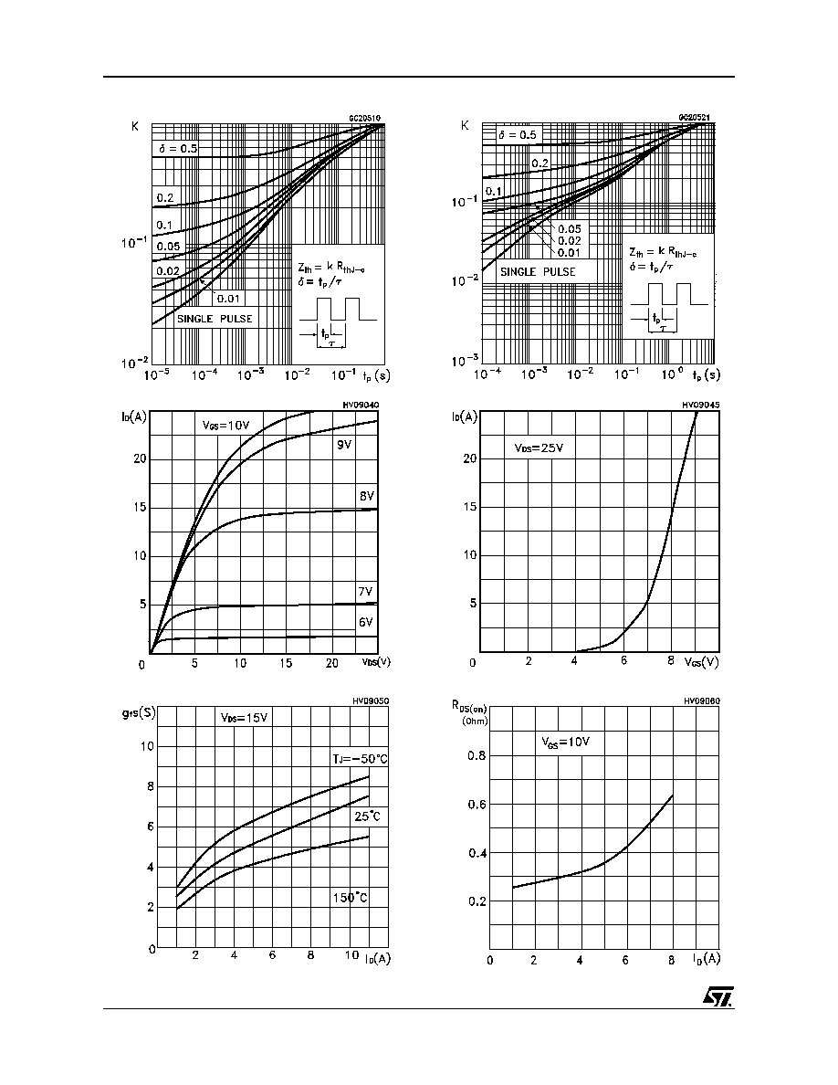
Transconductance
Static Drain-source On Resistance
Transfer Characteristics
Output Characteristics
Thermal Impedance for TO-220FP
Thermal Impedance for TO-220/D2PAK/I2PAK

5/12
STP11NM60 / STP11NM60FP / STB11NM60 / STB11NM60-1
Source-drain Diode Forward Characteristics
Normalized On Resistance vs Temperature
Normalized Gate Thereshold Voltage vs Temp.
Capacitance Variations
Gate Charge vs Gate-source Voltage