August 23, 1996
RF & MICROWAVE TRANSISTORS
UHF BASE STATION APPLICATIONS
.
470 MHZ
.
24 VOLTS
.
P
OUT
=
1.5 W WITH 13.0 dB MIN. GAIN
.
CLASS A
.
COMMON EMITTER
.
POWER SATURATION 2.2 W MIN.
P RELIMINARY DATA
DESCRIPTION
The SD1390 is a gold metallized NPN planar tran-
sistor using diffused emitter ballast resistors for
reliability and ruggedness.
The SD1390 is specifically designed as a low
power, high gain driver and can be operated in
Class A, B or C.
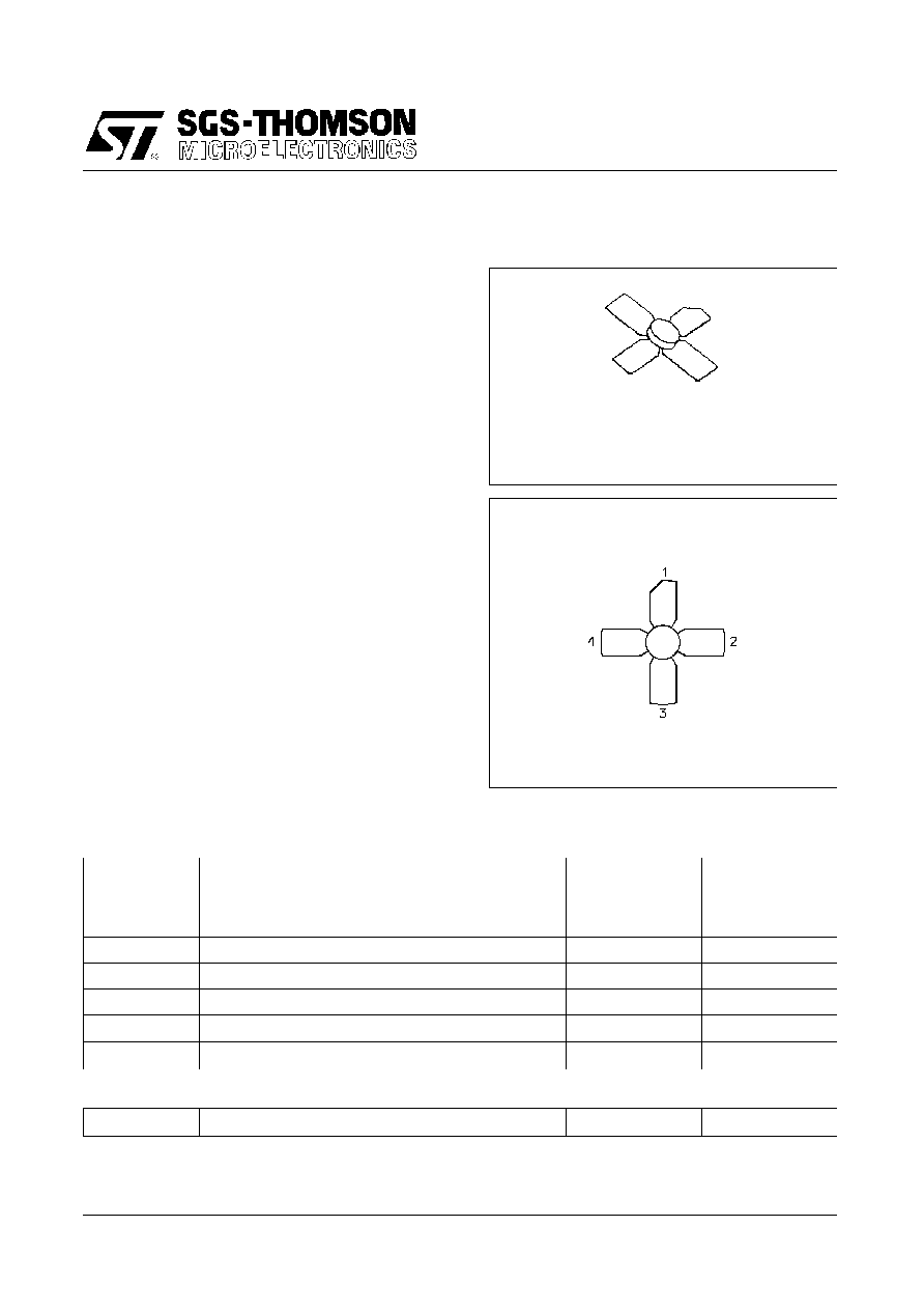
PIN CONNECTION
ABSOLUTE MAXIMUM RATINGS (T
case
=
25
∞
C)
Symbol
Parameter
Value
Un it
V
CBO
Collector-Base Voltage
40
V
V
CEO
Collector-Emitter Voltage
24
V
V
EBO
Emitter-Base Voltage
3.5
V
I
C
Collector Current
0.35
A
P
DISS
Power Dissipation (T
C
+75
∞
C)
8.33
W
T
J
Junction Temperature
+200
∞
C
T
STG
Storage Temperature
-
65 to +150
∞
C
R
TH(j- c)
Junction-Case Thermal Resistance
12
∞
C/W
SD1390
1. Collector
3. Base
2. Emitter
4. Emitter
THERMAL DATA
.28 0 x 4LS L (M1 2 3 )
O R DE R CODE
SD1390
BRANDING
SD1390
1/ 5
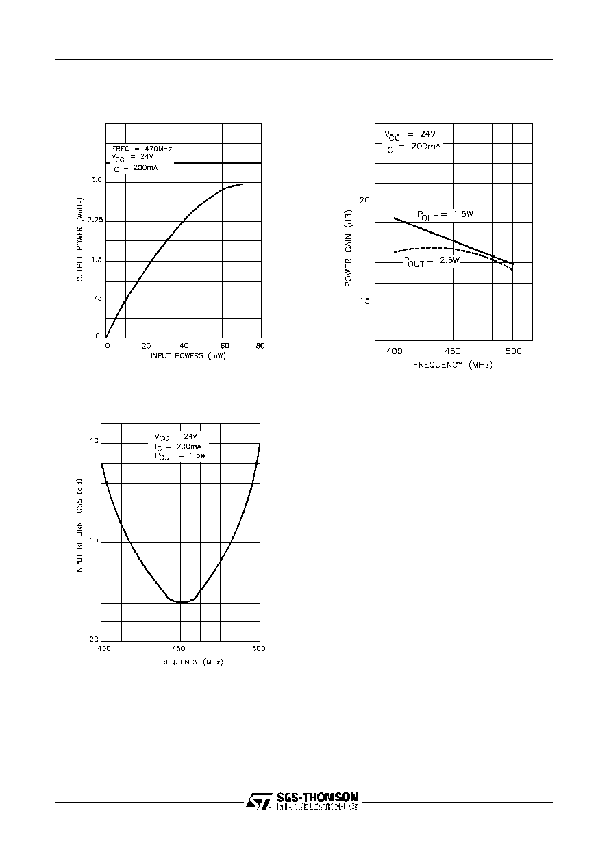
TYPICAL PERFORMANCE
INPUT RETURN LOSS vs FRE QUENCY
POWE R GAIN vs FREQUE NCY
OUTPUT POW ER vs INPUT POWE R
SD1390
3/ 5
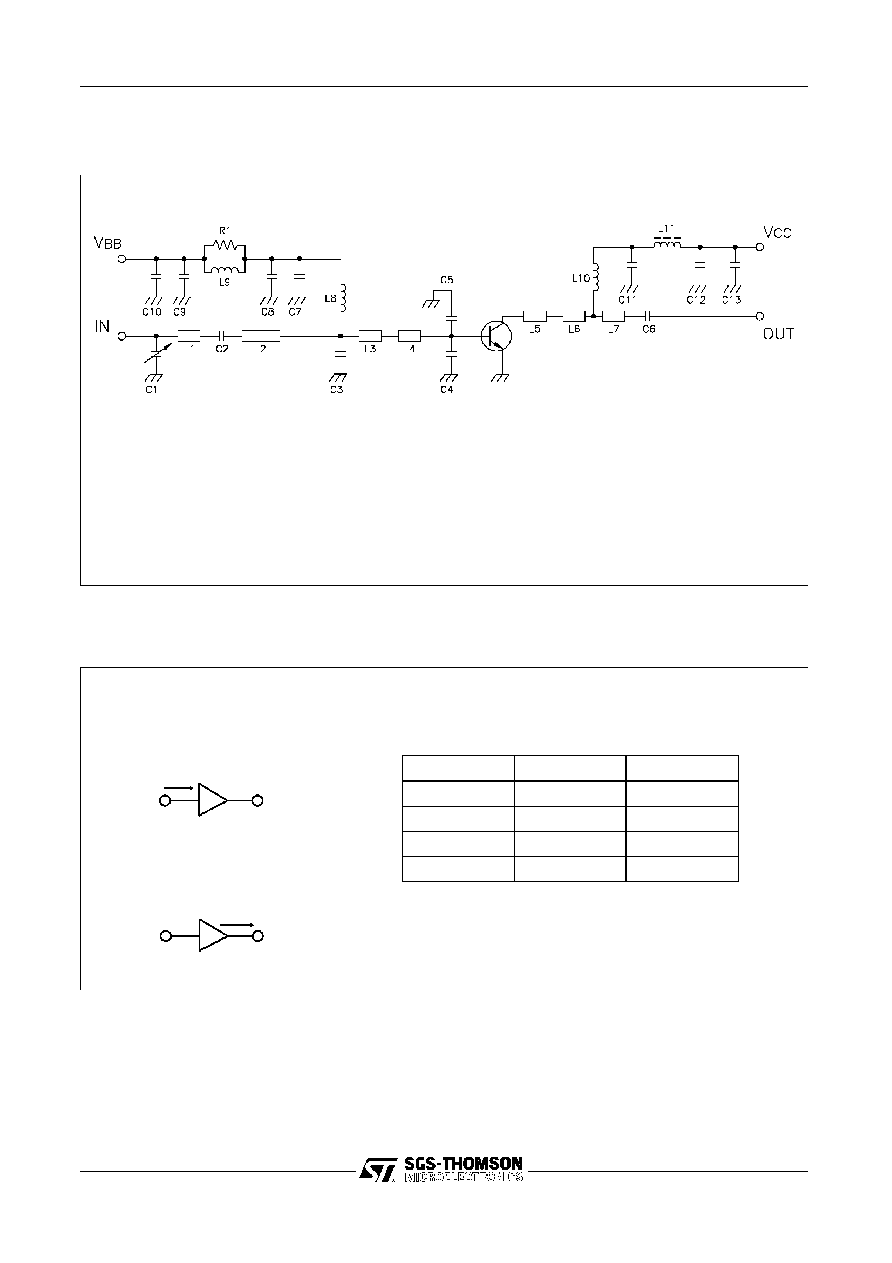
TYP ICAL COLLE CTOR LOAD
IMP E DANC E
TYP ICAL INP UT
IMP E DANCE
Z
IN
Z
CL
C1
:
Trim Capacitor GKU10056 2.8-10pf
C2, C6 :
Chip Capacitor LCC AC12CE221J / 220pf
C3
:
Chip Capacitor VITRAMON "High Q" / 15+4.7pf
C4,C5 :
Chip Capacitor LCC AC 12CE270J / 27 pf
C7,C9,C11:
C12
:
Chip Capacitor LCC AC20CD102K+AC12CE220J / 1nF+220 pf
C8,C10 :
C13
:
Tantle 10 mF, 35V
L1
:
Microstrip lin W = 2.1 mm, L = 10mm
L2
:
Microstrip line W = 1.0mm, L = 26mm
L3
:
Microstrip line W = 10mm, L = 10mm
L4
:
Microstrip line W = 8.0mm, L = 5mm
L5
:
Microstrip line W = 8.0mm, L = 5mm
L6
:
Microstrip line W = 1.0mm, L = 15mm
L7
:
Microstrip line W = 1.0mm, L = 30mm
L8
:
4 Tu rns ID = 2.5mm, 0.5mm Wire
L9
:
11 turns ID = 2. 5mm, 0.5 mm Wire
L10 :
2 Tu rns ID = 5.0mm, 1.0mm Wire
L11 :
Choke
R1
:
220 ohms - 1/4 Watts
IMPEDANCE DATA
FREQ.
Z
IN
(
)
Z
CL
(
)
400 MHz
2.8 + j 3.0
33 + j 47
430 MHz
2.6 + j 4.0
36 + j 49
470 MHz
2.4 + j 4.5
41 + j 52
500 MHz
2.0 + j 5.0
45 + j 54
TEST CIRCUIT
SD1390
4/5
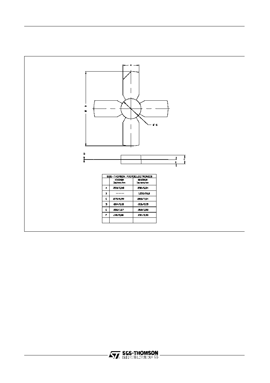
PACKAGE MECHANICAL DATA
Ref.: Dwg. No. 12-0123 rev. A
UDCS No. 1010947
Information furnished is believed to be accurate and reliable. However, SGS-THOMSON Microelectronics assumes no responsibility for the
consequences of use of such information nor for any infringement of patents or other rights of third parties which may result from its use.
No license is granted by implication or otherwise under any patent or patent rights of SGS-THOMSON Microelectronics. Specifications
mentioned in this publication are subject to change without notice. This publication supersedes and replaces all information previously
supplied. SGS-THOMSON Microelectronics products are not authorized for use as critical components in life support devices or systems
without express written approval of SGS-THOMSON Microelectronics.
©
1996 SGS-TH OMSON Microelectronics - All Rights Reserved
SGS-THOMSON Microelectronics GROUP OF COMPANIE S
Australia - Brazil - France - Germany - Hong Kong - Italy - Japan - Korea - Malaysia -
Malta - Morocco - The Netherlands - Singapore - Spain - Sweden - Switzerland - Taiwan -
Thailand - United Kingdom - U.S.A.
SD1390
5/ 5