
STP20N10
N - CHANNEL ENHANCEMENT MODE
POWER MOS TRANSISTOR
s
TYPICAL R
DS(on)
= 0.09
s
AVALANCHE RUGGED TECHNOLOGY
s
100% AVALANCHE TESTED
s
REPETITIVE AVALANCHE DATA AT 100
o
C
s
LOW GATE CHARGE
s
HIGH CURRENT CAPABILITY
s
175
o
C OPERATING TEMPERATURE
s
APPLICATION ORIENTED
CHARACTERIZATION
APPLICATIONS
s
HIGH CURRENT, HIGH SPEED SWITCHING
s
SOLENOID AND RELAY DRIVERS
s
REGULATORS
s
DC-DC & DC-AC CONVERTERS
s
MOTOR CONTROL, AUDIO AMPLIFIERS
s
AUTOMOTIVE ENVIRONMENT (INJECTION,
ABS, AIR-BAG, LAMPDRIVERS, Etc.)
INTERNAL SCHEMATIC DIAGRAM
TYPE
V
D SS
R
DS( on)
I
D
STP20N10
100 V
< 0.12
20 A
1
2
3
TO-220
December 1996
ABSOLUTE MAXIMUM RATINGS
Symbol
Parameter
Value
Unit
V
D S
Drain-source Voltage (V
GS
= 0)
100
V
V
DGR
Drain- gate Voltage (R
GS
= 20 k
)
100
V
V
GS
Gate-source Voltage
±
20
V
I
D
Drain Current (continuous) at T
c
= 25
o
C
20
A
I
D
Drain Current (continuous) at T
c
= 100
o
C
14
A
I
D M
(
∑
)
Drain Current (pulsed)
80
A
P
tot
Total Dissipation at T
c
= 25
o
C
105
W
Derating Factor
0.7
W/
o
C
T
stg
Storage Temperature
-65 to 175
o
C
T
j
Max. Operating Junction Temperature
175
o
C
(
∑
) Pulse width limited by safe operating area
1/9
THERMAL DATA
R
thj-case
R
thj- amb
R
thj- amb
T
l
Thermal Resistance Junction-case Max
Thermal Resistance Junction-ambient Max
Thermal Resistance Case-sink Typ
Maximum Lead Temperature For Soldering Purpose
1.43
62.5
0.5
300
o
C/W
o
C/W
o
C/W
o
C
AVALANCHE CHARACTERISTICS
Symbol
Parameter
Max Value
Unit
I
A R
Avalanche Current, Repetitive or Not-Repetitive
(pulse width limited by T
j
max,
< 1%)
20
A
E
AS
Single Pulse Avalanche Energy
(starting T
j
= 25
o
C, I
D
= I
AR
, V
D D
= 25 V)
60
mJ
E
AR
Repetitive Avalanche Energy
(pulse width limited by T
j
max,
< 1%)
15
mJ
I
A R
Avalanche Current, Repetitive or Not-Repetitive
(T
c
= 100
o
C, pulse width limited by T
j
max,
< 1%)
14
A
ELECTRICAL CHARACTERISTICS (T
case
= 25
o
C unless otherwise specified)
OFF
Symbol
Parameter
Test Conditions
Min.
Typ.
Max.
Unit
V
( BR) DSS
Drain-source
Breakdown Voltage
I
D
= 250
µ
A V
GS
= 0
100
V
I
DS S
Zero Gate Voltage
Drain Current (V
GS
= 0)
V
D S
= Max Rating
V
D S
= Max Rating x 0.8 T
c
= 125
o
C
1
10
µ
A
µ
A
I
GSS
Gate-body Leakage
Current (V
D S
= 0)
V
GS
=
±
20 V
±
100
nA
ON (
)
Symbol
Parameter
Test Conditions
Min.
Typ.
Max.
Unit
V
GS(th)
Gate Threshold Voltage V
D S
= V
GS
I
D
= 250
µ
A
2
2.9
4
V
R
DS( on)
Static Drain-source On
Resistance
V
GS
= 10V I
D
= 10 A
0.09
0.12
I
D( on)
On State Drain Current
V
D S
> I
D( on)
x R
D S(on) max
V
GS
= 10 V
20
A
DYNAMIC
Symbol
Parameter
Test Conditions
Min.
Typ.
Max.
Unit
g
fs
(
)
Forward
Transconductance
V
D S
> I
D( on)
x R
D S(on) max
I
D
= 10 A
7
12
S
C
iss
C
oss
C
rss
Input Capacitance
Output Capacitance
Reverse Transfer
Capacitance
V
D S
= 25 V f = 1 MHz V
GS
= 0
800
200
40
1100
300
60
pF
pF
pF
STP20N10
2/9
ELECTRICAL CHARACTERISTICS (continued)
SWITCHING ON
Symbol
Parameter
Test Conditions
Min.
Typ.
Max.
Unit
t
d(on)
t
r
Turn-on Time
Rise Time
V
D D
= 30 V I
D
= 3 A
R
G
= 50
V
GS
= 10 V
(see test circuit, figure 3)
25
75
35
110
ns
ns
(di/dt)
on
Turn-on Current Slope
V
D D
= 80 V I
D
= 20 A
R
G
= 50
V
GS
= 10 V
(see test circuit, figure 5)
300
A/
µ
s
Q
g
Q
gs
Q
gd
Total Gate Charge
Gate-Source Charge
Gate-Drain Charge
V
D D
= 80 V I
D
= 20 A V
GS
= 10 V
30
9
11
45
nC
nC
nC
SWITCHING OFF
Symbol
Parameter
Test Conditions
Min.
Typ.
Max.
Unit
t
r(Vof f)
t
f
t
c
Off-voltage Rise Time
Fall Time
Cross-over Time
V
D D
= 80 V I
D
= 20 A
R
G
= 50
V
GS
= 10 V
(see test circuit, figure 5)
70
55
130
100
80
185
ns
ns
ns
SOURCE DRAIN DIODE
Symbol
Parameter
Test Conditions
Min.
Typ.
Max.
Unit
I
S D
I
SDM
(
∑
)
Source-drain Current
Source-drain Current
(pulsed)
20
80
A
A
V
S D
(
)
Forward On Voltage
I
SD
= 20 A V
GS
= 0
1.6
V
t
rr
Q
r r
I
R RM
Reverse Recovery
Time
Reverse Recovery
Charge
Reverse Recovery
Current
I
SD
= 20 A di/dt = 100 A/
µ
s
V
D D
= 20 V T
j
= 150
o
C
(see test circuit, figure 5)
125
0.44
7
ns
µ
C
A
(
) Pulsed: Pulse duration = 300
µ
s, duty cycle 1.5 %
(
∑
) Pulse width limited by safe operating area
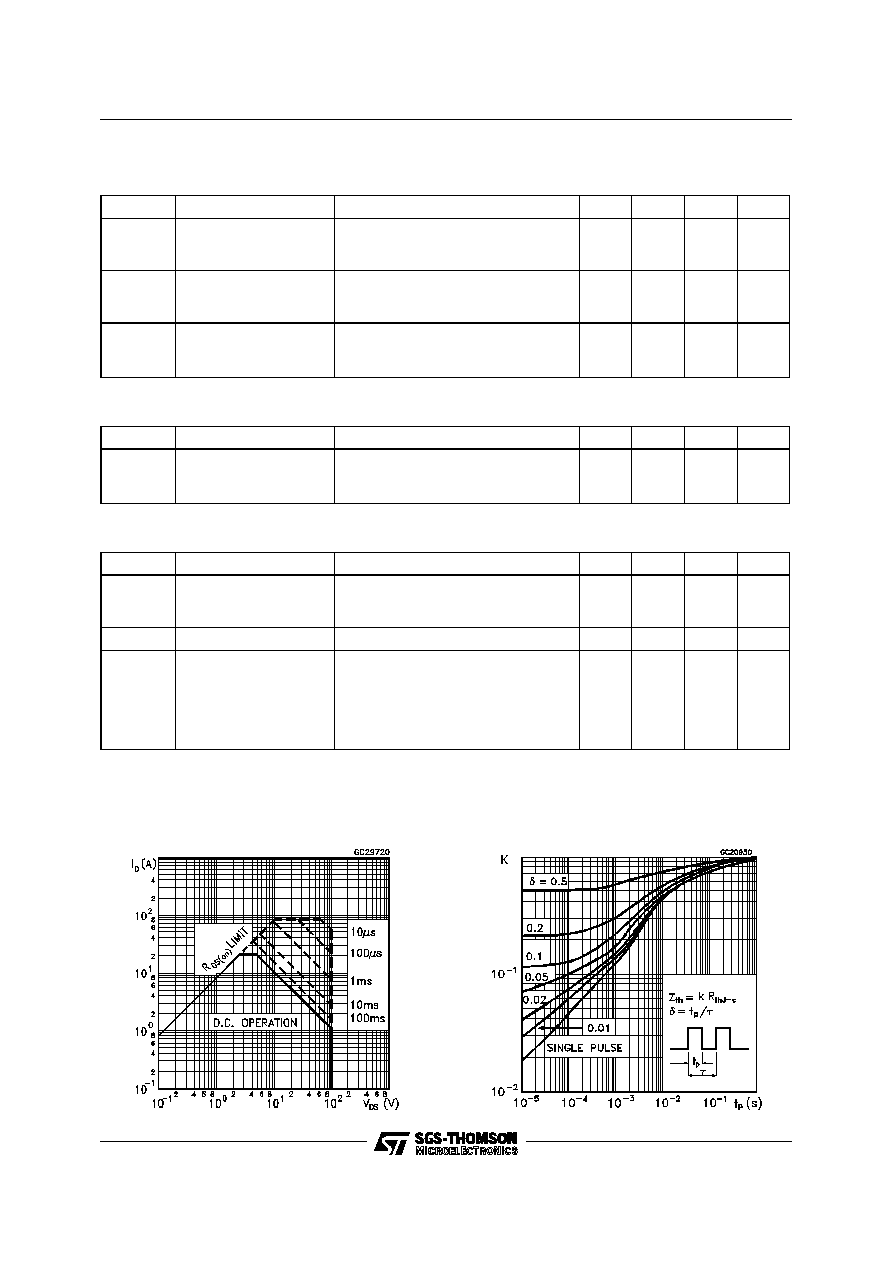
Safe Operating Areas
Thermal Impedance
STP20N10
3/9
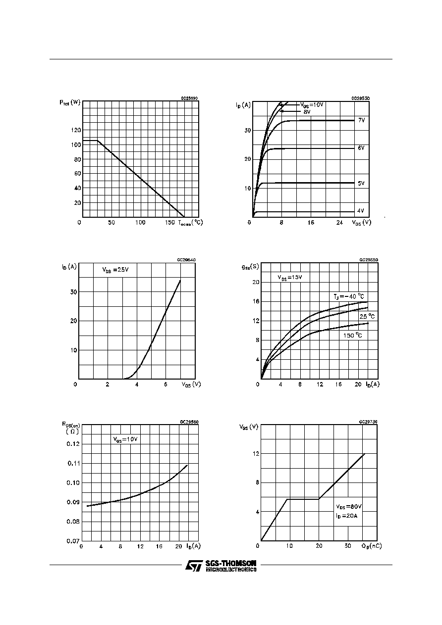
Derating Curve
Transfer Characteristics
Static Drain-source On Resistance
Output Characteristics
Transconductance
Gate Charge vs Gate-source Voltage
STP20N10
4/9
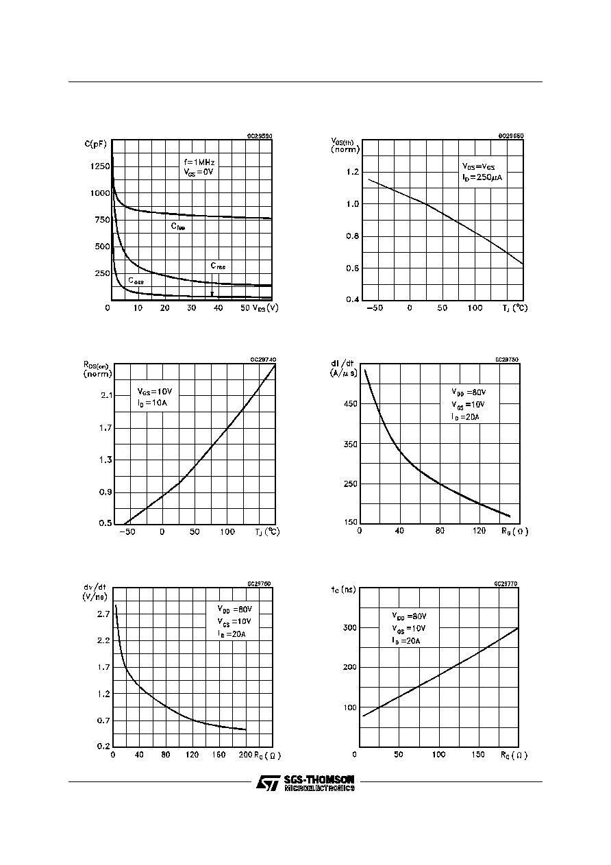
Capacitance Variations
Normalized Gate Threshold Voltage vs
Temperature
Normalized On Resistance vs Temperature
Turn-on Current Slope
Cross-over Time
Turn-off Drain-source Voltage Slope
STP20N10
5/9