
1/10
January 2002
STP22NS25Z
STB22NS25Z
N-CHANNEL 250V - 0.13
- 22A TO-220/D
2
PAK
Zener-Protected MESH OVERLAYTM MOSFET
(1) I
SD
22A, di/dt
200A/µs, V
DD
V
(BR)DSS
, T
j
T
JMAX.
INTERNAL SCHEMATIC DIAGRAM
s
TYPICAL R
DS
(on) = 0.13
s
EXTREMELY HIGH dv/dt CAPABILITY
s
100% AVALANCHE TESTED
DESCRIPTION
Using the latest high voltage MESH OVERLAYTM
process, STMicroelectronics has designed an ad-
vanced family of power MOSFETs with outstanding
performance. The new patented STrip layout cou-
pled with the Company's proprietary edge termina-
tion structure, makes it suitable in coverters for
lighting applications.
APPLICATIONS
s
HIGH CURRENT, HIGH SPEED SWITCHING
s
SWITH MODE POWER SUPPLIES (SMPS)
s
DC-DC CONVERTERS FOR TELECOM,
INDUSTRIAL, AND LIGHTING EQUIPMENT
ABSOLUTE MAXIMUM RATINGS
(∑)Pulse width limited by safe operating area
TYPE
V
DSS
R
DS(on)
I
D
STP22NS25Z
STB22NS25Z
250 V
250 V
< 0.15
< 0.15
22 A
22 A
Symbol
Parameter
Value
Unit
V
DS
Drain-source Voltage (V
GS
= 0)
250
V
V
DGR
Drain-gate Voltage (R
GS
= 20 k
)
250
V
V
GS
Gate- source Voltage
± 20
V
I
D
Drain Current (continuos) at T
C
= 25∞C
22
A
I
D
Drain Current (continuos) at T
C
= 100∞C
13.9
A
I
DM
(
l
)
Drain Current (pulsed)
88
A
P
TOT
Total Dissipation at T
C
= 25∞C
135
W
Derating Factor
1.07
W/∞C
V
ESD(G-S)
Gate source ESD(HBM-C=100pF, R=1.5K
)
2500
V
dv/dt (1)
Peak Diode Recovery voltage slope
5
V/ns
T
stg
Storage Temperature
≠55 to 150
∞C
T
j
Max. Operating Junction Temperature
TO-220
1
2
3
1
3
D
2
PAK

STP22NS25Z / STB22NS25Z
2/10
THERMAL DATA
AVALANCHE CHARACTERISTICS
ELECTRICAL CHARACTERISTICS (TCASE = 25 ∞C UNLESS OTHERWISE SPECIFIED)
OFF
ON
(1)
DYNAMIC
Rthj-case
Thermal Resistance Junction-case Max
0.93
∞C/W
Rthj-amb
Thermal Resistance Junction-ambient Max
62.5
∞C/W
T
l
Maximum Lead Temperature For Soldering Purpose
300
∞C
Symbol
Parameter
Max Value
Unit
I
AR
Avalanche Current, Repetitive or Not-Repetitive
(pulse width limited by T
j
max)
22
A
E
AS
Single Pulse Avalanche Energy
(starting T
j
= 25 ∞C, I
D
= I
AR
, V
DD
= 50 V, R
g
= 47 Ohm)
350
mJ
Symbol
Parameter
Test Conditions
Min.
Typ.
Max.
Unit
V
(BR)DSS
Drain-source
Breakdown Voltage
I
D
= 250 µA, V
GS
= 0
250
V
I
DSS
Zero Gate Voltage
Drain Current (V
GS
= 0)
V
DS
= Max Rating
10
µA
V
DS
= Max Rating, T
C
= 125 ∞C
100
µA
I
GSS
Gate-body Leakage
Current (V
DS
= 0)
V
GS
= ±18V
±10
µA
Symbol
Parameter
Test Conditions
Min.
Typ.
Max.
Unit
V
GS(th)
Gate Threshold Voltage
V
DS
= V
GS
, I
D
= 250µA
2
3
4
V
R
DS(on)
Static Drain-source On
Resistance
V
GS
= 10V, I
D
= 11 A
0.13
0.15
Symbol
Parameter
Test Conditions
Min.
Typ.
Max.
Unit
g
fs
(1)
Forward Transconductance
V
DS
> I
D(on)
x R
DS(on)max,
I
D
= 11A
22
S
C
iss
Input Capacitance
V
DS
= 25V, f = 1 MHz, V
GS
= 0
2400
pF
C
oss
Output Capacitance
340
pF
C
rss
Reverse Transfer
Capacitance
120
pF
3/10
STP22NS25Z / STB22NS25Z
ELECTRICAL CHARACTERISTICS (CONTINUED)
SWITCHING ON
SWITCHING OFF
SOURCE DRAIN DIODE
GATE-SOURCE ZENER DIODE
Note: 1. Pulsed: Pulse duration = 300 µs, duty cycle 1.5 %.
2. Pulse width limited by safe operating area.
PROTECTION FEATURES OF GATE-TO-SOURCE ZENER DIODES
The built-in back-to-back Zener diodes have specifically been designed to enhance not only the device's
ESD capability, but also to make them safely absorb possible voltage transients that may occasionally be
applied from gate to souce. In this respect the Zener voltage is appropriate to achieve an efficient and cost-
effective intervention to protect the device's integrity. These integrated Zener diodes thus avoid the usage
of external components.
Symbol
Parameter
Test Conditions
Min.
Typ.
Max.
Unit
t
d(on)
Turn-on Delay Time
V
DD
= 125 V, I
D
= 11 A
R
G
= 4.7
V
GS
= 10 V
(see test circuit, Figure 3)
20
ns
t
r
Rise Time
30
ns
Q
g
Total Gate Charge
V
DD
= 200V, I
D
= 20 A,
V
GS
= 10V
108
151
nC
Q
gs
Gate-Source Charge
11
nC
Q
gd
Gate-Drain Charge
40
nC
Symbol
Parameter
Test Conditions
Min.
Typ.
Max.
Unit
t
d(Voff)
t
f
Turn-off- Delay Time
Fall Time
V
DD
= 125V, I
D
= 11 A,
R
G
= 4.7
,
V
GS
= 10V
(see test circuit, Figure 3)
100
78
ns
ns
t
r(Voff)
t
f
t
c
Off-voltage Rise Time
Fall Time
Cross-over Time
V
clamp
= 200V, I
D
= 22 A,
R
G
= 4.7
,
V
GS
= 10V
(see test circuit, Figure 5)
37
65
110
ns
ns
ns
Symbol
Parameter
Test Conditions
Min.
Typ.
Max.
Unit
I
SD
Source-drain Current
22
A
I
SDM
(2)
Source-drain Current (pulsed)
88
A
V
SD
(1)
Forward On Voltage
I
SD
= 22 A, V
GS
= 0
1.6
V
t
rr
Reverse Recovery Time
I
SD
= 22 A, di/dt = 100A/µs
V
DD
= 50V, T
j
= 150∞C
(see test circuit, Figure 5)
292
ns
Q
rr
Reverse Recovery Charge
3065
nC
I
RRM
Reverse Recovery Current
21
A
Symbol
Parameter
Test Conditions
Min.
Typ.
Max.
Unit
BV
GSO
Gate-Source Breakdown
Voltage
Igs=± 500
µ
A (Open Drain)
20
V

STP22NS25Z / STB22NS25Z
4/10
Transconductance
Static Drain-source On Resistance
Transfer Characteristics
Output Characteristics
Thermal Impedance
Safe Operating Area

5/10
STP22NS25Z / STB22NS25Z
Normalized Gate Thereshold Voltage vs Temp.
Capacitance Variations
Normalized On Resistance vs Temperature
Source-drain Diode Forward Characteristics
Gate Charge vs Gate-source Voltage

STP22NS25Z / STB22NS25Z
6/10
Fig. 5: Test Circuit For Inductive Load Switching
And Diode Recovery Times
Fig. 4: Gate Charge test Circuit
Fig. 2: Unclamped Inductive Waveform
Fig. 1: Unclamped Inductive Load Test Circuit
Fig. 3: Switching Times Test Circuit For
Resistive Load
7/10
STP22NS25Z / STB22NS25Z
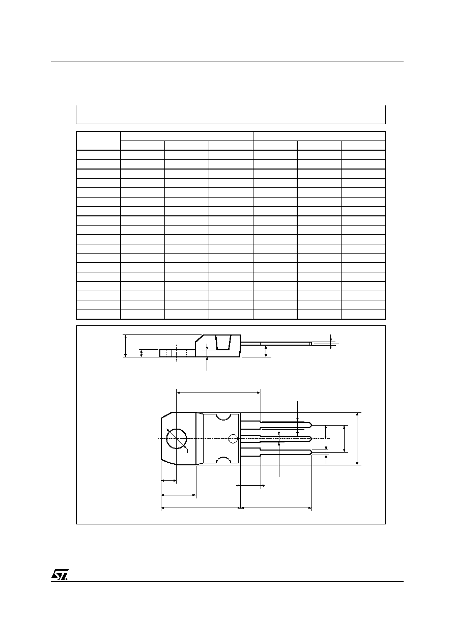
DIM.
mm
inch
MIN.
TYP.
MAX.
MIN.
TYP.
MAX.
A
4.40
4.60
0.173
0.181
C
1.23
1.32
0.048
0.051
D
2.40
2.72
0.094
0.107
D1
1.27
0.050
E
0.49
0.70
0.019
0.027
F
0.61
0.88
0.024
0.034
F1
1.14
1.70
0.044
0.067
F2
1.14
1.70
0.044
0.067
G
4.95
5.15
0.194
0.203
G1
2.4
2.7
0.094
0.106
H2
10.0
10.40
0.393
0.409
L2
16.4
0.645
L4
13.0
14.0
0.511
0.551
L5
2.65
2.95
0.104
0.116
L6
15.25
15.75
0.600
0.620
L7
6.2
6.6
0.244
0.260
L9
3.5
3.93
0.137
0.154
DIA.
3.75
3.85
0.147
0.151
L6
A
C
D
E
D1
F
G
L7
L2
Dia.
F1
L5
L4
H2
L9
F2
G1
TO-220 MECHANICAL DATA
P011C

STP22NS25Z / STB22NS25Z
8/10
1
DIM.
mm.
inch
MIN.
TYP
MAX.
MIN.
TYP.
MAX.
A
4.4
4.6
0.173
0.181
A1
2.49
2.69
0.098
0.106
A2
0.03
0.23
0.001
0.009
B
0.7
0.93
0.027
0.036
B2
1.14
1.7
0.044
0.067
C
0.45
0.6
0.017
0.023
C2
1.23
1.36
0.048
0.053
D
8.95
9.35
0.352
0.368
D1
8
0.315
E
10
10.4
0.393
E1
8.5
0.334
G
4.88
5.28
0.192
0.208
L
15
15.85
0.590
0.625
L2
1.27
1.4
0.050
0.055
L3
1.4
1.75
0.055
0.068
M
2.4
3.2
0.094
0.126
R
0.4
0.015
V2
0∫
8∫
D
2
PAK MECHANICAL DATA
3

9/10
STP22NS25Z / STB22NS25Z
TAPE AND REEL SHIPMENT (suffix "T4")*
TUBE SHIPMENT (no suffix)*
D
2
PAK FOOTPRINT
* on sales type
DIM.
mm
inch
MIN.
MAX.
MIN.
MAX.
A
330
12.992
B
1.5
0.059
C
12.8
13.2
0.504
0.520
D
20.2
0795
G
24.4
26.4
0.960
1.039
N
100
3.937
T
30.4
1.197
BASE QTY
BULK QTY
1000
1000
REEL MECHANICAL DATA
DIM.
mm
inch
MIN.
MAX.
MIN.
MAX.
A0
10.5
10.7
0.413
0.421
B0
15.7
15.9
0.618
0.626
D
1.5
1.6
0.059
0.063
D1
1.59
1.61
0.062
0.063
E
1.65
1.85
0.065
0.073
F
11.4
11.6
0.449
0.456
K0
4.8
5.0
0.189
0.197
P0
3.9
4.1
0.153
0.161
P1
11.9
12.1
0.468
0.476
P2
1.9
2.1
0.075
0.082
R
50
1.574
T
0.25
0.35
0.0098 0.0137
W
23.7
24.3
0.933
0.956
TAPE MECHANICAL DATA

STP22NS25Z / STB22NS25Z
10/10
Information furnished is believed to be accurate and reliable. However, STMicroelectronics assumes no responsibility for the consequences
of use of such information nor for any infringement of patents or other rights of third parties which may result from its use. No license is
granted by implication or otherwise under any patent or patent rights of STMicroelectronics. Specification mentioned in this publication are
subject to change without notice. This publication supersedes and replaces all information previously supplied. STMicroelectronics products
are not authorized for use as critical components in life support devices or systems without express written approval of STMicroelectronics.
The ST logo is a trademark of STMicroelectronics
© 2001 STMicroelectronics ≠ Printed in Italy ≠ All Rights Reserved
STMicroelectronics GROUP OF COMPANIES
Australia - Brazil - China - Finland - France - Germany - Hong Kong - India - Italy - Japan - Malaysia - Malta - Morocco -
Singapore - Spain - Sweden - Switzerland - United Kingdom - U.S.A.
http://www.st.com