 | –≠–ª–µ–∫—Ç—Ä–æ–Ω–Ω—ã–π –∫–æ–º–ø–æ–Ω–µ–Ω—Ç: STP36NF06 | –°–∫–∞—á–∞—Ç—å:  PDF PDF  ZIP ZIP |

1/9
October 2003
STP36NF06
STP36NF06FP
N-CHANNEL 60V - 0.032
- 30A TO-220/TO-220FP
STripFETTM II POWER MOSFET
s
TYPICAL R
DS
(on) = 0.032
s
EXCEPTIONAL dv/dt CAPABILITY
s
100% AVALANCHE TESTED
s
APPLICATION ORIENTED
CHARACTERIZATION
DESCRIPTION
This Power MOSFET is the latest development of
STMicroelectronis unique "Single Feature SizeTM"
strip-based process. The resulting transistor
shows extremely high packing density for low on-
resistance, rugged avalanche characteristics and
less critical alignment steps therefore a
remarkable manufacturing reproducibility.
APPLICATIONS
s
HIGH CURRENT, HIGH SWITCHING SPEED
TYPE
V
DSS
R
DS(on)
I
D
STP36NF06
STP36NF06FP
60 V
60 V
<0.040
<0.040
30 A
18 A
(*)
1
2
3
1
2
3
TO-220
TO-220FP
Ordering Information
ABSOLUTE MAXIMUM RATINGS
(
∑)
Pulse width limited by safe operating area.
(*) Current Limited by Package
(1) I
SD
36A, di/dt
400A/µs, V
DD
V
(BR)DSS
, T
j
T
JMAX
(2) Starting T
j
= 25
o
C, I
D
= 18 A, V
DD
= 45V
SALES TYPE
MARKING
PACKAGE
PACKAGING
STP36NF06
STP36NF06
TO-220
TUBE
STP36NF06FP
STP36NF06FP
TO-220FP
TUBE
Symbol
Parameter
Value
Unit
STP36NF06
STP36NF06FP
V
DS
Drain-source Voltage (V
GS
= 0)
60
V
V
DGR
Drain-gate Voltage (R
GS
= 20 k
)
60
V
V
GS
Gate- source Voltage
± 20
V
I
D
Drain Current (continuous) at T
C
= 25∞C
30
18
(*)
A
I
D
Drain Current (continuous) at T
C
= 100∞C
21
12
A
I
DM
(
∑)
Drain Current (pulsed)
120
72
A
P
tot
Total Dissipation at T
C
= 25∞C
70
25
W
Derating Factor
0.47
0.17
W/∞C
dv/dt
(1)
Peak Diode Recovery voltage slope
20
V/ns
E
AS (2)
Single Pulse Avalanche Energy
200
mJ
T
stg
Storage Temperature
-55 to 175
∞C
T
j
Max. Operating Junction Temperature
INTERNAL SCHEMATIC DIAGRAM
STP36NF06 STP36NF06FP
2/9
THERMAL DATA
ELECTRICAL CHARACTERISTICS (T
case
= 25 ∞C unless otherwise specified)
OFF
ON
(*)
DYNAMIC
TO-220
TO-220FP
Rthj-case
Thermal Resistance Junction-case
Max
2.14
6
∞C/W
Rthj-amb
T
l
Thermal Resistance Junction-ambient
Maximum Lead Temperature For Soldering Purpose
(1.6 mm from case, for 10 sec)
Max
62.5
300
∞C/W
∞C
Symbol
Parameter
Test Conditions
Min.
Typ.
Max.
Unit
V
(BR)DSS
Drain-source
Breakdown Voltage
I
D
= 250 µA, V
GS
= 0
60
V
I
DSS
Zero Gate Voltage
Drain Current (V
GS
= 0)
V
DS
= Max Rating
V
DS
= Max Rating T
C
= 125∞C
1
10
µA
µA
I
GSS
Gate-body Leakage
Current (V
DS
= 0)
V
GS
= ± 20 V
±100
nA
Symbol
Parameter
Test Conditions
Min.
Typ.
Max.
Unit
V
GS(th)
Gate Threshold Voltage
V
DS
= V
GS
I
D
= 250 µA
2
V
R
DS(on)
Static Drain-source On
Resistance
V
GS
= 10 V
I
D
= 15 A
0.032
0.040
Symbol
Parameter
Test Conditions
Min.
Typ.
Max.
Unit
g
fs (*)
Forward Transconductance
V
DS
= 25 V
I
D
= 15 A
12
S
C
iss
C
oss
C
rss
Input Capacitance
Output Capacitance
Reverse Transfer
Capacitance
V
DS
= 25V f = 1 MHz V
GS
= 0
690
170
68
pF
pF
pF
3/9
STP36NF06 STP36NF06FP
SWITCHING ON
SWITCHING OFF
SOURCE DRAIN DIODE
(*)
Pulsed: Pulse duration = 300 µs, duty cycle 1.5 %.
(
∑)
Pulse width limited by safe operating area.
Symbol
Parameter
Test Conditions
Min.
Typ.
Max.
Unit
t
d(on)
t
r
Turn-on Delay Time
Rise Time
V
DD
= 30 V
I
D
= 18 A
R
G
= 4.7
V
GS
= 10 V
(Resistive Load, Figure 3)
10
40
ns
ns
Q
g
Q
gs
Q
gd
Total Gate Charge
Gate-Source Charge
Gate-Drain Charge
V
DD
= 30 V I
D
= 36 A V
GS
= 10V
23
6
9
31
nC
nC
nC
Symbol
Parameter
Test Conditions
Min.
Typ.
Max.
Unit
t
d(off)
t
f
Turn-off Delay Time
Fall Time
V
DD
= 30 V
I
D
= 18 A
R
G
= 4.7
V
GS
=10 V
(Resistive Load, Figure 3)
27
9
ns
ns
Symbol
Parameter
Test Conditions
Min.
Typ.
Max.
Unit
I
SD
I
SDM
(
∑
)
Source-drain Current
Source-drain Current (pulsed)
30
120
A
A
V
SD
(*)
Forward On Voltage
I
SD
= 30 A
V
GS
= 0
1.5
V
t
rr
Q
rr
I
RRM
Reverse Recovery Time
Reverse Recovery Charge
Reverse Recovery Current
I
SD
= 30 A
di/dt = 100A/µs
V
DD
= 30 V
T
j
= 150∞C
(see test circuit, Figure 5)
65
155
4.8
ns
nC
A
ELECTRICAL CHARACTERISTICS (continued)
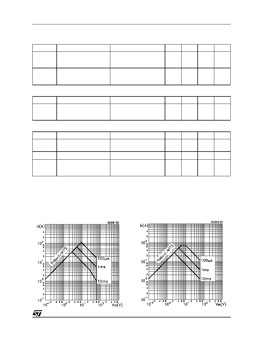
Safe Operating Area for TO-220
Safe Operating Area for TO-220FP

STP36NF06 STP36NF06FP
4/9
Thermal Impedance
Thermal Impedance for TO-220FP
Output Characteristics
Transfer Characteristics
Transconductance
Static Drain-source On Resistance
5/9
STP36NF06 STP36NF06FP
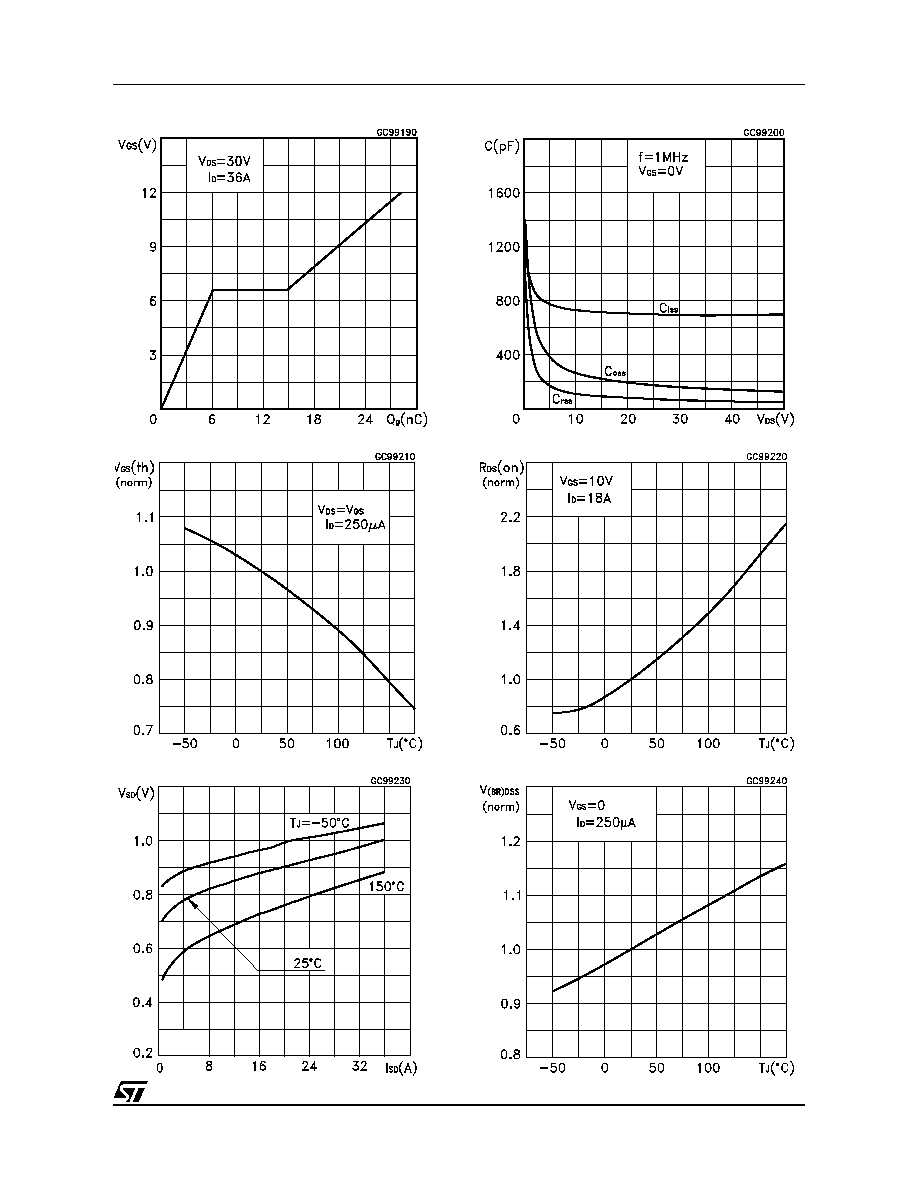
Gate Charge vs Gate-source Voltage
Capacitance Variations
Normalized Gate Threshold Voltage vs Temperature
Normalized on Resistance vs Temperature
Source-drain Diode Forward Characteristics
Normalized Breakdown Voltage Temperature