1/11
November 2002
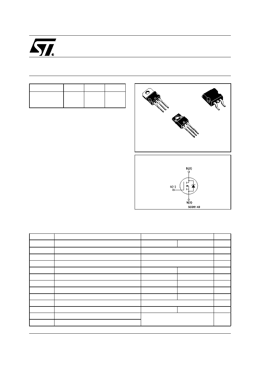
STP45NF3LL - STP45NF3LLFP
STB45NF3LL
N-CHANNEL 30V - 0.014
- 45A TO-220 - TO220FP - D
2
PAK
STripFET IITM POWER MOSFET
(1) Starting T
j
= 25∞C, I
D
= 22.5A, V
DD
= 24V
s
TYPICAL R
DS
(on) = 0.014
@4.5V
s
OPTIMAL RDS(ON) x Qg TRADE-OFF @ 4.5V
s
CONDUCTION LOSSES REDUCED
s
SWITCHING LOSSES REDUCED
s
ADD SUFFIX "T4" FOR ORDERING IN TAPE &
REEL
DESCRIPTION
This application specific Power MOSFET is the
third genaration of STMicroelectronics unique
"Single Feature Size
TM"
strip-based process. The
resulting transistor shows the best trade-off be-
tween on-resistance ang gate charge. When used
as high and low side in buck regulators, it gives the
best performance in terms of both conduction and
switching losses. This is extremely important for
motherboards where fast switching and high effi-
ciency are of paramount importance.
APPLICATIONS
s
SPECIFICALLY DESIGNED AND OPTIMISED
FOR HIGH EFFICIENCY DC/DC
CONVERTERS
ABSOLUTE MAXIMUM RATINGS
(
q
) Pulse width limited by safe operating area
TYPE
V
DSS
R
DS(on)
I
D
STP45NF3LL
STP45NF3LLFP
STB45NF3LL
30 V
30 V
30 V
<0.018
<0.018
<0.018
45 A
45 A
27 A
Symbol
Parameter
Value
Unit
TO-220/D
2
PAK
TO-220FP
V
DS
Drain-source Voltage (V
GS
= 0)
30
V
V
DGR
Drain-gate Voltage (R
GS
= 20 k
)
30
V
V
GS
Gate- source Voltage
± 16
V
I
D
Drain Current (continuous) at T
C
= 25∞C
45
27
A
I
D
Drain Current (continuous) at T
C
= 100∞C
32
19
A
I
DM
( )
Drain Current (pulsed)
180
108
A
P
TOT
Total Dissipation at T
C
= 25∞C
70
25
W
Derating Factor
0.46
0.167
W/∞C
E
AS
(1)
Single Pulse Avalanche Energy
241
mJ
Viso
Insulation Withstand Voltage (DC)
--
2500
V
T
stg
Storage Temperature
≠ 55 to 175
∞C
T
j
Max. Operating Junction Temperature
D
2
PAK
1
3
1
2
3
TO-220
1
2
3
TO-220FP
INTERNAL SCHEMATIC DIAGRAM

STP45NF3LL - STB45NF3LL
2/11
THERMAL DATA
ELECTRICAL CHARACTERISTICS (TCASE = 25 ∞C UNLESS OTHERWISE SPECIFIED)
OFF
ON (1)
DYNAMIC
TO-220
D
2
PAK
TO-220FP
Rthj-case
Thermal Resistance Junction-case Max
2.14
6
∞C/W
Rthj-amb
Thermal Resistance Junction-ambient Max
62.5
∞C/W
T
l
Maximum Lead Temperature For Soldering Purpose
300
∞C
Symbol
Parameter
Test Conditions
Min.
Typ.
Max.
Unit
V
(BR)DSS
Drain-source
Breakdown Voltage
I
D
= 250 µA, V
GS
= 0
30
V
I
DSS
Zero Gate Voltage
Drain Current (V
GS
= 0)
V
DS
= Max Rating
1
µA
V
DS
= Max Rating, T
C
= 125 ∞C
10
µA
I
GSS
Gate-body Leakage
Current (V
DS
= 0)
V
GS
= ± 16 V
±100
nA
Symbol
Parameter
Test Conditions
Min.
Typ.
Max.
Unit
V
GS(th)
Gate Threshold Voltage
V
DS
= V
GS
, I
D
= 250µA
1
V
R
DS(on)
Static Drain-source On
Resistance
V
GS
= 10 V, I
D
= 22.5 A
0.014
0.018
V
GS
= 4.5V, I
D
= 22.5 A
0.016
0.020
Symbol
Parameter
Test Conditions
Min.
Typ.
Max.
Unit
g
fs
(1)
Forward Transconductance
V
DS
=15 V
,
I
D
= 22.5 A
20
S
C
iss
Input Capacitance
V
DS
= 25V, f = 1 MHz, V
GS
= 0
800
pF
C
oss
Output Capacitance
250
pF
C
rss
Reverse Transfer
Capacitance
60
pF

3/11
STP45NF3LL - STB45NF3LL
ELECTRICAL CHARACTERISTICS (CONTINUED)
SWITCHING ON
SWITCHING OFF
SOURCE DRAIN DIODE
Note: 1. Pulsed: Pulse duration = 300 µs, duty cycle 1.5 %.
2. Pulse width limited by safe operating area.
Symbol
Parameter
Test Conditions
Min.
Typ.
Max.
Unit
t
d(on)
Turn-on Delay Time
V
DD
= 15 V, I
D
= 22.5A
R
G
= 4.7
V
GS
= 4.5V
(Resistive Load, see Fig. 3)
17
ns
t
r
Rise Time
100
ns
Q
g
Q
gs
Q
gd
Total Gate Charge
Gate-Source Charge
Gate-Drain Charge
V
DD
= 24V, I
D
= 45A,
V
GS
= 5V
12.5
4.6
5.2
17
nC
nC
nC
Symbol
Parameter
Test Conditions
Min.
Typ.
Max.
Unit
t
d(off)
t
f
Turn-off-Delay Time
Fall Time
V
DD
= 15V, I
D
= 22.5A,
R
G
= 4.7
,
V
GS
= 4.5V
(Resistive Load, see Fig. 3)
20
21
ns
ns
Symbol
Parameter
Test Conditions
Min.
Typ.
Max.
Unit
I
SD
Source-drain Current
45
A
I
SDM
(2)
Source-drain Current (pulsed)
180
A
V
SD
(1)
Forward On Voltage
I
SD
= 45A, V
GS
= 0
1.3
V
t
rr
Q
rr
I
RRM
Reverse Recovery Time
Reverse Recovery Charge
Reverse Recovery Current
I
SD
= 45A, di/dt = 100A/µs,
V
DD
= 15V, T
j
= 150∞C
(see test circuit, Figure 5)
35
44
2.5
ns
nC
A
Safe Operating Area for TO-220/D2PAK
Thermal Impedance for TO-220/D2PAK

STP45NF3LL - STB45NF3LL
4/11
Thermal Impedance for TO-220FP
Safe Operating Area for TO-220FP
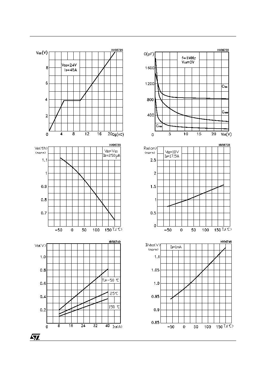
Transconductance
Static Drain-source On Resistance
Transfer Characteristics
Output Characteristics
5/11
STP45NF3LL - STB45NF3LL
Source-drain Diode Forward Characteristics
Normalized Breakdown Voltage vs Tj
Normalized On Resistance vs Temperature
Normalized Gate Thereshold Voltage vs Temp.
Gate Charge vs Gate-source Voltage
Capacitance Variations