 | –≠–ª–µ–∫—Ç—Ä–æ–Ω–Ω—ã–π –∫–æ–º–ø–æ–Ω–µ–Ω—Ç: STP50NE08 | –°–∫–∞—á–∞—Ç—å:  PDF PDF  ZIP ZIP |

STP50NE08
N - CHANNEL ENHANCEMENT MODE
" SINGLE FEATURE SIZE
TM
" POWER MOSFET
s
TYPICAL R
DS(on)
= 0.020
s
EXCEPTIONAL dv/dt CAPABILITY
s
100% AVALANCHE TESTED
s
LOW GATE CHARGE AT 100
o
C
s
APPLICATION ORIENTED
CHARACTERIZATION
DESCRIPTION
This Power MOSFET is the latest development of
SGS-THOMSON unique "Single Feature Size
TM
"
strip-based
process. The resulting transistor
shows extremely high packing density for low
on-resistance, rugged avalanche characteristics
and less critical alignment steps therefore a
remarkable manufacturing reproducibility.
APPLICATIONS
s
HIGH CURRENT, HIGH SPEED SWITCHING
s
SOLENOID AND RELAY DRIVERS
s
MOTOR CONTROL, AUDIO AMPLIFIERS
s
DC-DC & DC-AC CONVERTERS
s
AUTOMOTIVE ENVIRONMENT (INJECTION,
ABS, AIR-BAG, LAMPDRIVERS, Etc.)
INTERNAL SCHEMATIC DIAGRAM
March 1998
1
2
3
TO-220
ABSOLUTE MAXIMUM RATINGS
Symbol
Parameter
Value
Uni t
V
DS
Drain-source Volt age (V
GS
= 0)
80
V
V
DGR
Drain- gate Voltage (R
GS
= 20 k
)
80
V
V
G S
Gat e-source Voltage
±
20
V
I
D
Drain Current (continuous) at T
c
= 25
o
C
50
A
I
D
Drain Current (continuous) at T
c
= 100
o
C
35
A
I
DM
(
∑
)
Drain Current (pulsed)
200
A
P
t ot
Tot al Dissipation at T
c
= 25
o
C
150
W
Derating F act or
1
W/
o
C
dv/dt (
1
)
Peak Diode Recovery voltage slope
6
V/ ns
T
stg
Storage T emperat ure
-65 to 175
o
C
T
j
Max. O perating Junction Temperature
175
o
C
(
∑
) Pulse width limited by safe operating area
(
1
) I
SD
50 A, di/dt
300 A/
µ
s, V
DD
V
(BR)DSS
, T
j
T
JMAX
TYPE
V
DSS
R
DS(on)
I
D
ST P50NE08
80 V
<0.024
50 A
1/8

THERMAL DATA
R
t hj-ca se
Rthj -am b
R
thc- si nk
T
l
Thermal Resistance Junction-case
Max
Thermal Resistance Junction-ambient
Max
Thermal Resistance Case-sink
Typ
Maximum Lead Temperature For Soldering Purpose
1
62.5
0.5
300
o
C/ W
oC/W
o
C/ W
o
C
AVALANCHE CHARACTERISTICS
Symb ol
Parameter
Max Valu e
Uni t
I
AR
Avalanche Current, Repetitive or Not -Repet itive
(pulse width limited by T
j
max,
< 1%)
50
A
E
AS
Single Pulse Avalanche Energy
(starting T
j
= 25
o
C, I
D
= I
AR
, V
DD
= 50 V)
300
mJ
ELECTRICAL CHARACTERISTICS (T
case
= 25
o
C unless otherwise specified)
OFF
Symb ol
Parameter
Test Cond ition s
Mi n.
Typ .
Max.
Un it
V
(BR)DSS
Drain-source
Breakdown Volt age
I
D
= 250
µ
A
V
GS
= 0
80
V
I
DSS
Zero G ate Voltage
Drain Current (V
GS
= 0)
V
DS
= Max Rating
V
DS
= Max Rating
T
c
= 125
o
C
1
10
µ
A
µ
A
I
GSS
Gate-body Leakage
Current (V
DS
= 0)
V
G S
=
±
20 V
±
100
nA
ON (
)
Symb ol
Parameter
Test Cond ition s
Mi n.
Typ .
Max.
Un it
V
GS(th)
Gate Threshold
Voltage
V
DS
= V
GS
I
D
= 250
µ
A
2
3
4
V
R
DS( on)
St atic Drain-source On
Resistance
V
G S
= 10V
I
D
= 25 A
0.020
0.024
m
I
D(o n)
On St ate Drain Current
V
DS
> I
D(on)
x R
DS(on) max
V
G S
= 10 V
50
A
DYNAMIC
Symb ol
Parameter
Test Cond ition s
Mi n.
Typ .
Max.
Un it
g
fs
(
)
Forward
Transconduct ance
V
DS
> I
D(on)
x R
DS(on) max
I
D
=25 A
20
35
S
C
iss
C
oss
C
rss
Input Capacitance
Output Capacit ance
Reverse T ransfer
Capacitance
V
DS
= 25 V
f = 1 MHz
V
GS
= 0
3850
480
105
5100
650
140
pF
pF
pF
STP50NE08
2/8

ELECTRICAL CHARACTERISTICS (continued)
SWITCHING ON
Symb ol
Parameter
Test Cond ition s
Mi n.
Typ .
Max.
Un it
t
d(on)
t
r
Turn-on Time
Rise Time
V
DD
= 40 V
I
D
= 25 A
R
G
=4.7
V
GS
= 10 V
(see test circuit, figure 3)
37
95
50
130
ns
ns
Q
g
Q
gs
Q
gd
Total Gate Charge
Gate-Source Charge
Gate-Drain Charge
V
DD
= 64 V
I
D
= 50 A
V
GS
= 10 V
85
19
28
110
nC
nC
nC
SWITCHING OFF
Symb ol
Parameter
Test Cond ition s
Mi n.
Typ .
Max.
Un it
t
r(Vof f)
t
f
t
c
Of f-voltage Rise Time
Fall Time
Cross-over Time
V
DD
= 64 V
I
D
= 50 A
R
G
=4.7
V
GS
= 10 V
(see test circuit, figure 5)
12
30
50
17
40
68
ns
ns
ns
SOURCE DRAIN DIODE
Symb ol
Parameter
Test Cond ition s
Mi n.
Typ .
Max.
Un it
I
SD
I
SDM
(
∑
)
Source-drain Current
Source-drain Current
(pulsed)
50
200
A
A
V
SD
(
)
Forward On Voltage
I
SD
= 50 A
V
GS
= 0
1.5
V
t
rr
Q
rr
I
RRM
Reverse Recovery
Time
Reverse Recovery
Charge
Reverse Recovery
Current
I
SD
= 50 A
di/ dt = 100 A/
µ
s
V
DD
= 30 V
T
j
= 150
o
C
(see test circuit, figure 5)
100
400
8
ns
nC
A
(
) Pulsed: Pulse duration = 300
µ
s, duty cycle 1.5 %
(
∑
) Pulse width limited by safe operating area
Safe Operating Area
Thermal Impedance
STP50NE08
3/8

Output Characteristics
Transconductance
Gate Charge vs Gate-source Voltage
Transfer Characteristics
Static Drain-source On Resistance
Capacitance Variations
STP50NE08
4/8
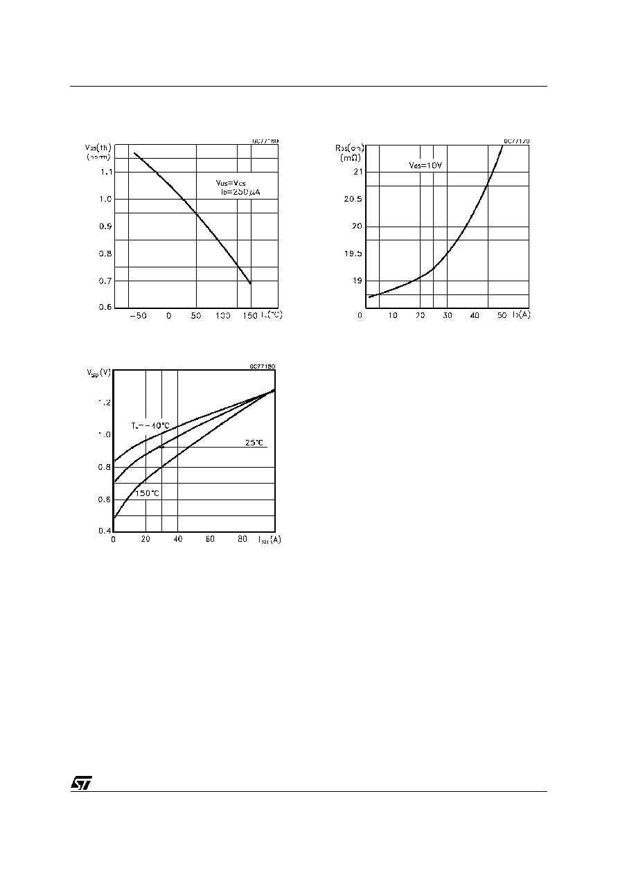
Normalized Gate Threshold Voltage vs
Temperature
Source-drain Diode Forward Characteristics
Normalized On Resistance vs Temperature
STP50NE08
5/8