
STP55NE06L
STP55NE06LFP
N - CHANNEL ENHANCEMENT MODE
" SINGLE FEATURE SIZE
TM
" POWER MOSFET
s
TYPICAL R
DS(on)
= 0.018
s
EXCEPTIONAL dV/dt CAPABILTY
s
100% AVALANCHE TESTED
s
LOW GATE CHARGE 100
o
C
s
HIGH dV/dt CAPABILITY
s
APPLICATION ORIENTED
CHARACTERIZATION
DESCRIPTION
This Power Mosfet is the latest development of
SGS-THOMSON unique "Single Feature Size"
process whereby a single body is implanted on a
strip layout structure. The resulting transistor
shows extremely high packing density for low on-
resistance, rugged avalanche characteristics and
less critical alignment steps therefore a remark-
able manufacturing reproducibility.
APPLICATIONS
s
DC MOTOR CONTROL
s
DC-DC & DC-AC CONVERTERS
s
SYNCHRONOUS RECTIFICATION
INTERNAL SCHEMATIC DIAGRAM
ABSOLUTE MAXIMUM RATINGS
Symbol
Parameter
Valu e
Uni t
STP55NE06L
ST P55NE06LFP
V
DS
Drain-source Voltage (V
GS
= 0)
60
V
V
DGR
Drain- gate Volt age (R
GS
= 20 k
)
60
V
V
G S
Gat e-source Volt age
±
15
V
I
D
Drain Current (continuous) at T
c
= 25
o
C
55
28
A
I
D
Drain Current (continuous) at T
c
= 100
o
C
39
20
A
I
DM
(
∑
)
Drain Current (pulsed)
220
220
A
P
t ot
Tot al Dissipation at T
c
= 25
o
C
130
35
W
Derating Factor
0. 86
0.23
W/
o
C
V
ISO
Insulation W it hstand Voltage (DC)
2000
V
dV/ dt
Peak Diode Recovery voltage slope
7
V/ ns
T
stg
Storage Temperature
-65 to 175
o
C
T
j
Max. O perat ing Junction Temperature
175
o
C
(
∑
) Pulse width limited by safe operating area
(
1
) I
SD
55 A, di/dt
300 A/
µ
s, V
DD
V
(BR)DSS
, T
j
T
JMAX
TYPE
V
DSS
R
DS(on)
I
D
STP55NE06L
STP55NE06LF P
60 V
60 V
< 0.022
< 0.022
55 A
28 A
December 1997
TO-220
TO220FP
1
2
3
1
2
3
1/6

THERMAL DATA
T O-220
T O-220F P
R
t hj-ca se
Thermal Resist ance Junction-case
Max
1. 15
4.28
o
C/ W
R
t hj- amb
R
thc- si nk
T
l
Thermal Resist ance Junction-ambient
Max
Thermal Resist ance Case-sink
Typ
Maximum Lead Temperature For Soldering Purpose
62.5
0.5
300
o
C/ W
o
C/ W
o
C
AVALANCHE CHARACTERISTICS
Symb ol
Parameter
Max Valu e
Uni t
I
AR
Avalanche Current, Repetitive or Not -Repetitive
(pulse width limited by T
j
max,
< 1%)
55
A
E
AS
Single Pulse Avalanche Energy
(starting T
j
= 25
o
C, I
D
= I
AR
, V
DD
= 25 V)
250
mJ
ELECTRICAL CHARACTERISTICS (T
case
= 25
o
C unless otherwise specified)
OFF
Symb ol
Parameter
Test Cond ition s
Mi n.
Typ .
Max.
Un it
V
(BR)DSS
Drain-source
Breakdown Volt age
I
D
= 250
µ
A
V
G S
= 0
60
V
I
DSS
Zero Gat e Voltage
Drain Current (V
GS
= 0)
V
DS
= Max Rating
V
DS
= Max Rating
T
c
= 125
o
C
1
10
µ
A
µ
A
I
GSS
Gate-body Leakage
Current (V
DS
= 0)
V
G S
=
±
15 V
±
100
nA
ON (
)
Symb ol
Parameter
Test Cond ition s
Mi n.
Typ .
Max.
Un it
V
GS(th)
Gate T hreshold Voltage V
DS
= V
GS
I
D
= 250
µ
A
1
1.7
2.5
V
R
DS( on)
St atic Drain-source O n
Resistance
V
G S
= 5 V
I
D
= 27.5 A
V
G S
= 10 V
I
D
= 27.5 A
0.022
0.019
0. 028
0. 022
I
D(o n)
On Stat e Drain Current
V
DS
> I
D(on)
x R
DS(on) max
V
G S
= 10 V
55
A
DYNAMIC
Symb ol
Parameter
Test Cond ition s
Mi n.
Typ .
Max.
Un it
g
fs
(
)
Forward
Transconductance
V
DS
> I
D(on)
x R
DS(on) max
I
D
=27.5 A
20
30
S
C
iss
C
oss
C
rss
Input Capacitance
Output Capacit ance
Reverse Transfer
Capacitance
V
DS
= 25 V
f = 1 MHz
V
GS
= 0
2800
375
100
3750
500
140
pF
pF
pF
STP55NE06LFP
2/6

ELECTRICAL CHARACTERISTICS (continued)
SWITCHING ON
Symb ol
Parameter
Test Cond ition s
Mi n.
Typ .
Max.
Un it
t
d(on)
t
r
Turn-on T ime
Rise Time
V
DD
= 30 V
I
D
= 27.5 A
R
G
=4.7
V
GS
= 5 V
40
100
55
140
ns
ns
Q
g
Q
gs
Q
gd
Total G ate Charge
Gate-Source Charge
Gate-Drain Charge
V
DD
= 48 V
I
D
= 55 A
V
G S
= 5 V
40
13
20
55
nC
nC
nC
SWITCHING OFF
Symb ol
Parameter
Test Cond ition s
Mi n.
Typ .
Max.
Un it
t
r(Vof f)
t
f
t
c
Of f-voltage Rise Time
Fall Time
Cross-over T ime
V
DD
= 48 V
I
D
= 55 A
R
G
=4.7
V
G S
= 5 V
25
40
65
35
55
90
ns
ns
ns
SOURCE DRAIN DIODE
Symb ol
Parameter
Test Cond ition s
Mi n.
Typ .
Max.
Un it
I
SD
I
SDM
(
∑
)
Source-drain Current
Source-drain Current
(pulsed)
55
220
A
A
V
SD
(
)
Forward O n Volt age
I
SD
= 55 A
V
GS
= 0
1.5
V
t
rr
Q
rr
I
RRM
Reverse Recovery
Time
Reverse Recovery
Charge
Reverse Recovery
Current
I
SD
= 55 A
di/ dt = 100 A/
µ
s
V
DD
= 30 V
T
j
= 150
o
C
65
180
5.5
ns
nC
A
(
) Pulsed: Pulse duration = 300
µ
s, duty cycle 1.5 %
(
∑
) Pulse width limited by safe operating area
STP55NE06LFP
3/6

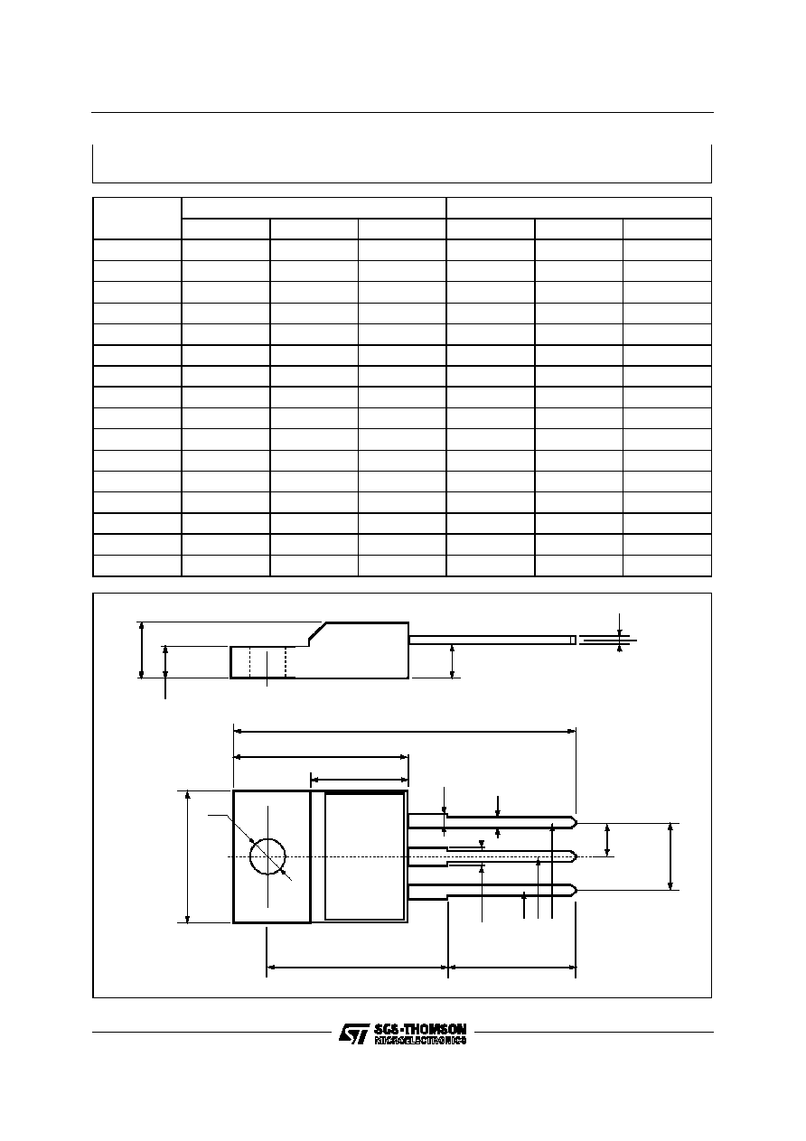
DIM.
mm
inch
MIN.
TYP.
MAX.
MIN.
TYP.
MAX.
A
4.40
4.60
0.173
0.181
C
1.23
1.32
0.048
0.051
D
2.40
2.72
0.094
0.107
D1
1.27
0.050
E
0.49
0.70
0.019
0.027
F
0.61
0.88
0.024
0.034
F1
1.14
1.70
0.044
0.067
F2
1.14
1.70
0.044
0.067
G
4.95
5.15
0.194
0.203
G1
2.4
2.7
0.094
0.106
H2
10.0
10.40
0.393
0.409
L2
16.4
0.645
L4
13.0
14.0
0.511
0.551
L5
2.65
2.95
0.104
0.116
L6
15.25
15.75
0.600
0.620
L7
6.2
6.6
0.244
0.260
L9
3.5
3.93
0.137
0.154
DIA.
3.75
3.85
0.147
0.151
L6
A
C
D
E
D1
F
G
L7
L2
Dia.
F1
L5
L4
H2
L9
F2
G1
TO-220 MECHANICAL DATA
P011C
STP55NE06LFP
4/6
DIM.
mm
inch
MIN.
TYP.
MAX.
MIN.
TYP.
MAX.
A
4.4
4.6
0.173
0.181
B
2.5
2.7
0.098
0.106
D
2.5
2.75
0.098
0.108
E
0.45
0.7
0.017
0.027
F
0.75
1
0.030
0.039
F1
1.15
1.7
0.045
0.067
F2
1.15
1.7
0.045
0.067
G
4.95
5.2
0.195
0.204
G1
2.4
2.7
0.094
0.106
H
10
10.4
0.393
0.409
L2
16
0.630
L3
28.6
30.6
1.126
1.204
L4
9.8
10.6
0.385
0.417
L6
15.9
16.4
0.626
0.645
L7
9
9.3
0.354
0.366
ÿ
3
3.2
0.118
0.126
L2
A
B
D
E
H
G
L6
Ø
F
L3
G1
1 2 3
F2
F1
L7
L4
TO-220FP MECHANICAL DATA
STP55NE06LFP
5/6