 | ÐлекÑÑоннÑй компоненÑ: STP5NA60 | СкаÑаÑÑ:  PDF PDF  ZIP ZIP |
Äîêóìåíòàöèÿ è îïèñàíèÿ www.docs.chipfind.ru
STP5NA60
STP5NA60FI
N - CHANNEL ENHANCEMENT MODE
FAST POWER MOS TRANSISTOR
s
TYPICAL R
DS(on)
= 1.35
s
±
30V GATE TO SOURCE VOLTAGE RATING
s
100% AVALANCHE TESTED
s
REPETITIVE AVALANCHE DATA AT 100
o
C
s
LOW INTRINSIC CAPACITANCES
s
GATE GHARGE MINIMIZED
s
REDUCED THRESHOLD VOLTAGE SPREAD
DESCRIPTION
This series of POWER MOSFETS represents the
most advanced high voltage technology. The
optimized
cell
layout
coupled
with
a
new
proprietary edge termination concur to give the
device low R
DS(on)
and gate charge, unequalled
ruggedness and superior switching performance.
APPLICATIONS
s
HIGH CURRENT, HIGH SPEED SWITCHING
s
SWITCH MODE POWER SUPPLIES (SMPS)
s
DC-AC CONVERTERS FOR WELDING
EQUIPMENT AND UNINTERRUPTIBLE
POWER SUPPLIES AND MOTOR DRIVE
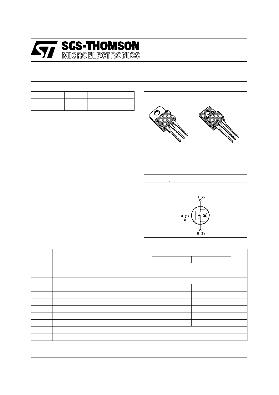
INTERNAL SCHEMATIC DIAGRAM
TYPE
V
DSS
R
DS ( on)
I
D
STP5NA60
STP5NA60FI
600 V
600 V
< 1. 6
< 1. 6
5.3 A
3.4 A
1
2
3
TO-220
ISOWATT220
November 1996
ABSOLUTE MAXIMUM RATINGS
Symbol
Parameter
Val ue
Unit
STP5NA60
STP5NA60FI
V
D S
Drain-source Voltage (V
GS
= 0)
600
V
V
DG R
Drain-gate Volt age (R
G S
= 20 k
)
600
V
V
GS
Gate-source Voltage
±
30
V
I
D
Drain Current (cont inuous) at T
c
= 25
o
C
5.3
3.4
A
I
D
Drain Current (cont inuous) at T
c
= 100
o
C
3.5
2.3
A
I
D M
(
·
)
Drain Current (pulsed)
21
21
A
P
tot
Total Dissipation at T
c
= 25
o
C
110
45
W
Derating Factor
0. 88
0.36
W/
o
C
V
ISO
I nsulat ion Withstand Voltage (DC)
2000
V
T
stg
St orage Temperat ure
-65 to 150
o
C
T
j
Max. Operat ing Junction Temperature
150
o
C
(
·
) Pulse width limited by safe operating area
1
2
3
1/10
THERMAL DATA
TO-220
ISOWATT220
R
thj-cas e
Thermal Resist ance Junct ion-case
Max
1.14
2. 78
o
C/W
R
thj- amb
R
t hc- sin k
T
l
Thermal Resist ance Junct ion-ambient
Max
Thermal Resist ance Case-sink
Typ
Maximum Lead Temperature For Soldering Purpose
62.5
0.5
300
o
C/W
o
C/W
o
C
AVALANCHE CHARACTERISTICS
Symbol
Parameter
Max Value
Uni t
I
A R
Avalanche Current, Repetitive or Not-Repetitive
(pulse width limited by T
j
max,
< 1%)
5.3
A
E
AS
Single Pulse Avalanche Energy
(st arting T
j
= 25
o
C, I
D
= I
AR
, V
D D
= 50 V)
140
mJ
E
AR
Repet itive Avalanche Energy
(pulse width limited by T
j
max,
< 1%)
6
mJ
I
A R
Avalanche Current, Repetitive or Not-Repetitive
(T
c
= 100
o
C, pulse width limited by T
j
max,
< 1%)
3.5
A
ELECTRICAL CHARACTERISTICS (T
case
= 25
o
C unless otherwise specified)
OFF
Symbol
Parameter
Test Condi tions
Mi n.
Typ.
Max.
Unit
V
( BR)DSS
Drain-source
Breakdown Voltage
I
D
= 250
µ
A
V
G S
= 0
600
V
I
DS S
Zero Gate Volt age
Drain Current (V
GS
= 0)
V
DS
= Max Rating
V
DS
= Max Rating x 0.8
T
c
= 125
o
C
25
250
µ
A
µ
A
I
G SS
Gate-body Leakage
Current (V
D S
= 0)
V
GS
=
±
30 V
±
100
nA
ON (
)
Symbol
Parameter
Test Condi tions
Mi n.
Typ.
Max.
Unit
V
G S(th)
Gate Threshold Voltage V
DS
= V
GS
I
D
= 250
µ
A
2. 25
3
3. 75
V
R
DS( on)
St atic Drain-source On
Resist ance
V
GS
= 10V
I
D
= 2.6 A
1.35
1.6
I
D( on)
On St ate Drain Current
V
DS
> I
D( on)
x R
D S(on) max
V
GS
= 10 V
5.3
A
DYNAMIC
Symbol
Parameter
Test Condi tions
Mi n.
Typ.
Max.
Unit
g
fs
(
)
Forward
Transconductance
V
DS
> I
D( on)
x R
D S(on) max
I
D
= 2. 6 A
2.7
4.7
S
C
iss
C
oss
C
rss
I nput Capacitance
Output Capacit ance
Reverse Transfer
Capacitance
V
DS
= 25 V
f = 1 MHz
V
G S
= 0
925
130
32
1210
175
45
pF
pF
pF
STP5NA60/FI
2/10
ELECTRICAL CHARACTERISTICS (continued)
SWITCHING ON
Symbol
Parameter
Test Condi tions
Mi n.
Typ.
Max.
Unit
t
d(on)
t
r
Turn-on Time
Rise Time
V
DD
= 300 V
I
D
= 2.5 A
R
G
= 47
V
GS
= 10 V
(see test circuit, figure 3)
28
75
40
100
ns
ns
(di/dt)
on
Turn-on Current Slope
V
DD
= 480 V
I
D
= 5 A
R
G
= 47
V
GS
= 10 V
(see test circuit, figure 5)
215
A/
µ
s
Q
g
Q
gs
Q
gd
Total Gate Charge
Gate-Source Charge
Gate-Drain Charge
V
DD
= 480 V
I
D
= 5 A
V
GS
= 10 V
45
8
19
60
nC
nC
nC
SWITCHING OFF
Symbol
Parameter
Test Condi tions
Mi n.
Typ.
Max.
Unit
t
r(Vof f)
t
f
t
c
Of f-voltage Rise Time
Fall Time
Cross-over Time
V
DD
= 480 V
I
D
= 5 A
R
G
= 47
V
GS
= 10 V
(see test circuit, figure 5)
60
18
95
85
27
130
ns
ns
ns
SOURCE DRAIN DIODE
Symbol
Parameter
Test Condi tions
Mi n.
Typ.
Max.
Unit
I
S D
I
SD M
(
·
)
Source-drain Current
Source-drain Current
(pulsed)
5.3
21
A
A
V
S D
(
)
Forward On Volt age
I
SD
= 5.3 A
V
GS
= 0
1.6
V
t
rr
Q
rr
I
RRM
Reverse Recovery
Time
Reverse Recovery
Charge
Reverse Recovery
Current
I
SD
= 5 A
di/dt = 100 A/
µ
s
V
DD
= 100 V
T
j
= 150
o
C
(see test circuit, figure 5)
490
7.1
29
ns
µ
C
A
(
) Pulsed: Pulse duration = 300
µ
s, duty cycle 1.5 %
(
·
) Pulse width limited by safe operating area
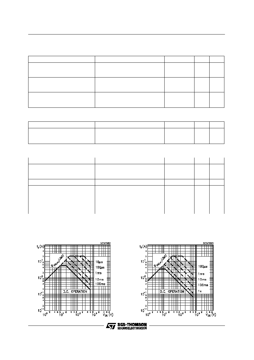
Safe Operating Areas for TO-220
Safe Operating Areas for ISOWATT220
STP5NA60/FI
3/10
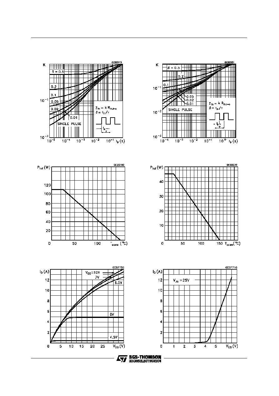
Thermal Impedeance For TO-220
Derating Curve For TO-220
Output Characteristics
Thermal Impedance For ISOWATT220
Derating Curve For ISOWATT220
Transfer Characteristics
STP5NA60/FI
4/10
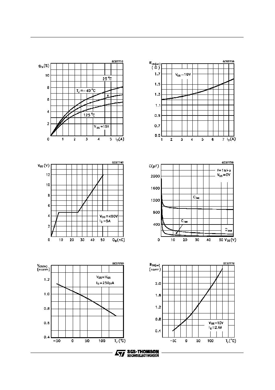
Transconductance
Static Drain-source On Resistance
Gate Charge vs Gate-source Voltage
Capacitance Variations
Normalized On Resistance vs Temperature
Normalized Gate Threshold Voltage vs
Temperature
STP5NA60/FI
5/10