STP6NB80
STP6NB80FP
N - CHANNEL 800V - 1.6
- 5.7A - TO-220/TO-220FP
PowerMESH
TM
MOSFET
PRELIMINARY DATA
s
TYPICAL R
DS(on)
= 1.6
s
EXTREMELY HIGH dv/dt CAPABILITY
s
100% AVALANCHE TESTED
s
VERY LOW INTRINSIC CAPACITANCES
s
GATE CHARGE MINIMIZED
DESCRIPTION
Using the latest high voltage MESH OVERLAY
TM
process, STMicroelectronics has designed an
advanced family
of
power MOSFETs with
outstanding performances. The
new
patent
pending strip layout coupled with the Company's
proprietary edge termination structure, gives the
lowest RDS(on) per area, exceptional avalanche
and dv/dt capabilities and unrivalled gate charge
and switching characteristics.
APPLICATIONS
s
HIGH CURRENT, HIGH SPEED SWITCHING
s
SWITCH MODE POWER SUPPLIES (SMPS)
s
DC-AC CONVERTERS FOR WELDING
EQUIPMENT AND UNINTERRUPTIBLE
POWER SUPPLIES AND MOTOR DRIVE
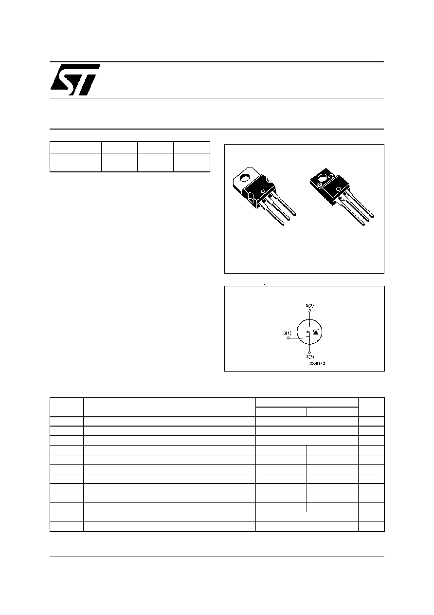
INTERNAL SCHEMATIC DIAGRAM
September 1998
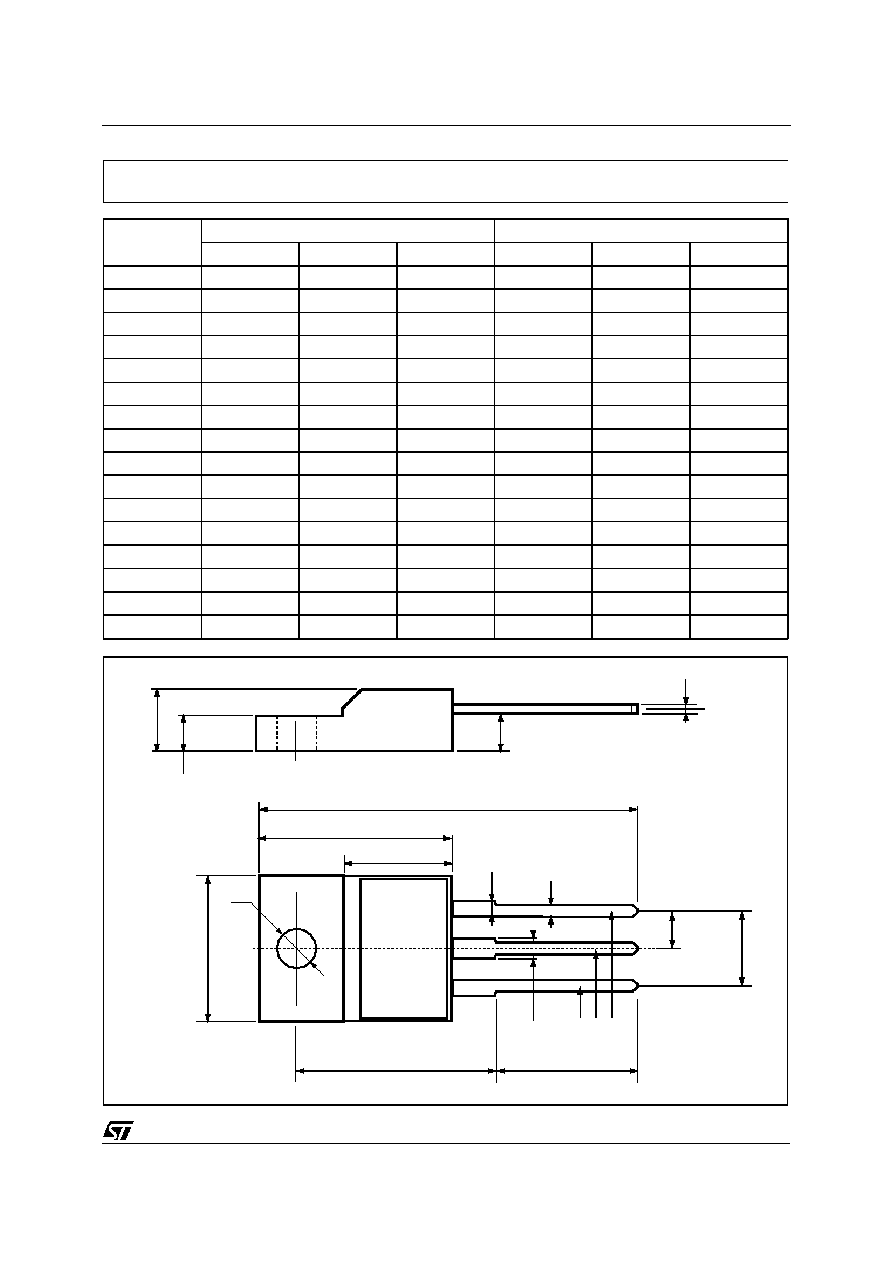
TO-220
TO-220FP
1
2
3
1
2
3
ABSOLUTE MAXIMUM RATINGS
Symbol
Parameter
Value
Un it
ST P6NB80
STP6NB80F P
V
DS
Drain-source Voltage (V
G S
= 0)
800
V
V
DGR
Drain- gate Voltage (R
GS
= 20 k
)
800
V
V
GS
G ate-source Volt age
±
30
V
I
D
Drain Current (continuous) at T
c
= 25
o
C
5.7
5.7(*)
A
I
D
Drain Current (continuous) at T
c
= 100
o
C
3.6
2
A
I
DM
(
∑
)
Drain Current (pulsed)
22.8
22.8
A
P
tot
T otal Dissipation at T
c
= 25
o
C
125
40
W
Derating F actor
1.0
0.32
W /
o
C
dv/dt (
1
)
Peak Diode Recovery voltage slope
4
4
V/ns
V
ISO
I nsulation W ithstand Voltage (DC)
2000
V
T
s tg
Storage Temperature
-65 to 150
o
C
T
j
Max. Operating Junction T emperature
150
o
C
(
∑
) Pulse width limited by safe operating area
(
1
) I
SD
5.76 A, di/dt
200 A/
µ
s, V
DD
V
(BR)DSS
, Tj
T
JMAX
(
*) Limited only maximum temperature allowed
TYPE
V
DSS
R
DS(on)
I
D
ST P6NB80
ST P6NB80FP
800 V
800 V
< 1.9
< 1.9
5.7 A
5.7 A
1/6

THERMAL DATA
TO-220
TO220-FP
R
thj -case
Thermal Resistance Junction-case
Max
1.0
3.1
o
C/W
R
thj -amb
R
thc-sink
T
l
Thermal Resistance Junction-ambient
Max
Thermal Resistance Case-sink
T yp
Maximum Lead T emperature For Soldering Purpose
62.5
0.5
300
o
C/W
o
C/W
o
C
AVALANCHE CHARACTERISTICS
Symbo l
Parameter
Max Value
Unit
I
AR
Avalanche Current , Repet itive or Not -Repetit ive
(pulse widt h limited by T
j
max)
5.7
A
E
AS
Single Pulse Avalanche Energy
(starting T
j
= 25
o
C, I
D
= I
AR
, V
DD
= 50 V)
314
mJ
ELECTRICAL CHARACTERISTICS (T
case
= 25
o
C unless otherwise specified)
OFF
Symbo l
Parameter
Test Con ditions
Min.
Typ.
Max.
Unit
V
(BR)DSS
Drain-source
Breakdown Voltage
I
D
= 250
µ
A
V
GS
= 0
800
V
I
DSS
Zero Gat e Voltage
Drain Current (V
GS
= 0)
V
DS
= Max Rat ing
V
DS
= Max Rat ing
T
c
= 125
o
C
1
50
µ
A
µ
A
I
G SS
Gat e-body Leakage
Current (V
DS
= 0)
V
GS
=
±
30 V
±
100
nA
ON (
)
Symbo l
Parameter
Test Con ditions
Min.
Typ.
Max.
Unit
V
G S(th)
Gat e Threshold Voltage V
DS
= V
GS
I
D
= 250
µ
A
3
4
5
V
R
DS(on)
Static Drain-source On
Resist ance
V
GS
= 10V
I
D
= 3 A
1.6
1. 9
I
D(o n)
On State Drain Current
V
DS
> I
D(o n)
x R
DS(on )ma x
V
GS
= 10 V
5. 7
A
DYNAMIC
Symbo l
Parameter
Test Con ditions
Min.
Typ.
Max.
Unit
g
f s
(
)
Forward
Transconductance
V
DS
> I
D(o n)
x R
DS(on )ma x
I
D
= 3 A
2. 5
4.5
S
C
iss
C
os s
C
rss
Input Capacitance
Out put Capacitance
Reverse Transfer
Capacitance
V
DS
= 25 V
f = 1 MHz
V
GS
= 0
1250
145
16
1625
190
21
pF
pF
pF
STP6NB80/FP
2/6

ELECTRICAL CHARACTERISTICS (continued)
SWITCHING ON
Symbo l
Parameter
Test Con ditions
Min.
Typ.
Max.
Unit
t
d(on)
t
r
Turn-on Time
Rise Time
V
DD
= 400 V
I
D
= 3 A
R
G
= 4.7
V
GS
= 10 V
19
9
27
13
ns
ns
Q
g
Q
gs
Q
gd
Tot al Gate Charge
Gat e-Source Charge
Gat e-Drain Charge
V
DD
= 640 V
I
D
= 6 A V
GS
= 10 V
33
11
14
47
nC
nC
nC
SWITCHING OFF
Symbo l
Parameter
Test Con ditions
Min.
Typ.
Max.
Unit
t
r (Voff)
t
f
t
c
Off -volt age Rise Time
Fall Time
Cross-over Time
V
DD
= 640V
I
D
= 6 A
R
G
= 4.7
V
G S
= 10 V
11
9
16
16
13
23
ns
ns
ns
SOURCE DRAIN DIODE
Symbo l
Parameter
Test Con ditions
Min.
Typ.
Max.
Unit
I
SD
I
SDM
(
∑
)
Source-drain Current
Source-drain Current
(pulsed)
5. 7
22. 8
A
A
V
SD
(
)
Forward On Voltage
I
SD
= 6 A
V
GS
= 0
1. 6
V
t
rr
Q
rr
I
RRM
Reverse Recovery
Time
Reverse Recovery
Charge
Reverse Recovery
Current
I
SD
= 6 A
di/dt = 100 A/
µ
s
V
DD
= 100 V
T
j
= 150
o
C
700
5.8
16.5
ns
µ
C
A
(
) Pulsed: Pulse duration = 300
µ
s, duty cycle 1.5 %
(
∑
) Pulse width limited by safe operating area
STP6NB80/FP
3/6