1/10
STPR1020CB/CG/CT/CF/CFP/CR
Æ
August 2002- Ed: 2E
ULTRA-FAST RECOVERY RECTIFIER DIODES
s
SUITED FOR SMPS
s
LOW LOSSES
s
LOW FORWARD AND REVERSE RECOVERY
TIME
s
HIGH SURGE CURRENT CAPABILITY
s
INSULATED PACKAGES: ISOWATT220AB /
TO-220FPAB
Insulation Voltage = 2000V DC
Capacitance = 12 pF
FEATURES
Symbol
Parameter
Value
Unit
V
RRM
Repetitive peak reverse voltage
200
V
I
F(RMS)
RMS forward
current
D
2
PAK / TO-220AB / ISOWATT220AB /
TO-220FPAB / I
2
PAK
10
A
DPAK
7
A
I
F(AV)
Average forward
current
= 0.5
D
2
PAK / DPAK
TO-220AB / I
2
PAK
Tc=125∞C
Per diode
5
A
ISOWATT220AB
Tc=115∞C
Per device
10
TO-220FPAB
Tc=110∞C
Per device
10
I
FSM
Surge non repetitive forward current
tp=10ms sinusoidal
50
A
T
stg
Storage temperature range
- 65 to + 150
∞
C
ABSOLUTE MAXIMUM (limiting values, per diode)
A1
A2
K
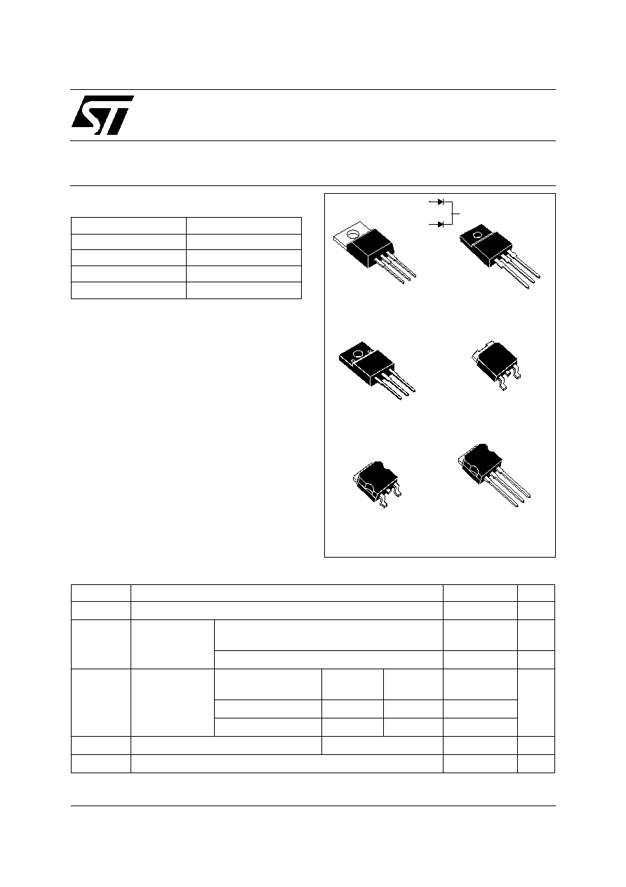
TO-220AB
STPR1020CT
A1
K
A2
K
A1
A2
ISOWATT220AB
STPR1020CF
Dual center tap rectifier suited for Switched Mode
Power Supplies and high frequency DC to DC
converters.
Packaged in DPAK, D
2
PAK, I
2
PAK, TO-220AB,
TO-220FPAB or ISOWATT220AB, this device is
intended for use in low voltage, high frequency
inverters, free wheeling and polarity protection
applications.
DESCRIPTION
I
F(AV)
2 x 5 A
V
RRM
200 V
Tj (max)
150∞C
V
F
(max)
0.99 V
trr (max)
30 ns
MAIN PRODUCTS CHARACTERISTICS
K
K
A1
A2
DPAK
STPR1020CB
K
A1
A2
D
2
PAK
STPR1020CG
A1
A2
K
TO-220FPAB
STPR1020CFP
A1
A2
K
I
2
PAK
STPR1020CR

STPR1020CB/CG/CT/CF/CFP/CR
2/10
Symbol
Parameters
Test conditions
Min.
Typ.
Max.
Unit
I
R
*
Reverse leakage
current
T
j
= 25∞C
V
R
= V
RRM
50
µ
A
T
j
= 100∞C
0.6
mA
V
F **
Forward voltage
drop
T
j
= 125
∞
C
I
F
= 5 A
0.8
0.99
V
T
j
= 125
∞
C
I
F
= 10 A
0.95
1.20
T
j
= 25∞C
I
F
= 10 A
1.25
Pulse test : * tp = 5 ms,
< 2 %
** tp = 380
µ
s,
< 2 %
To evaluate the conduction losses use the following equation :
P = 0.78 x I
F(AV)
+ 0.042 x I
F
2
(RMS)
STATIC ELECTRICAL CHARACTERISTICS (per diode)
Symbol
Test conditions
Min.
Typ.
Max.
Unit
trr
T
j
= 25∞C
I
F
= 0.5A
I
R
= 1A
Irr = 0.25A
30
ns
tfr
T
j
= 25
∞
C
I
F
= 1A
V
FR
= 1.1 x V
F
max
dI
F
/dt = 50 A/
µ
s
20
ns
V
FP
T
j
= 25
∞
C
I
F
= 1A
dI
F
/dt = 50 A/
µ
s
3
V
RECOVERY CHARACTERISTICS
Symbol
Parameter
Value
Unit
R
th (j-c)
Junction to case
TO-220AB / D
2
PAK / DPAK
I
2
PAK
Per diode
4.0
∞
C/W
Total
2.4
ISOWATT220AB
Per diode
6.0
Total
4.0
TO-220FPAB
Per diode
6.5
Total
5
R
th (c)
Coupling
TO-220AB / D
2
PAK / DPAK / I
2
PAK
0.7
ISOWATT220AB
2.0
TO-220FPAB
3.5
When diodes 1 and 2 are used simultaneously :
Tj(diode 1) = P(diode 1) x Rth(j-c) (Per diode) + P(diode 2) x Rth(c)
THERMAL RESISTANCES

STPR1020CB/CG/CT/CF/CFP/CR
3/10
0.0
0.1
0.2
0.3
0.4
0.5
0.6
0.7
0.8
0.9
1.0
0
5
10
15
20
25
30
35
40
45
50
IM(A)
P=2.5W
P=7.5W
P=10W
P=5W
T
=tp/T
tp
Fig. 2: Peak current versus form factor (per diode).
0.0 0.5 1.0 1.5 2.0 2.5 3.0 3.5 4.0 4.5 5.0 5.5 6.0
0
1
2
3
4
5
6
7
IF(av) (A)
PF(av)(W)
= 0.05
= 0.1
= 0.2
= 0.5
= 1
T
=tp/T
tp
Fig. 1: Average forward power dissipation versus
average forward current (per diode).
0
25
50
75
100
125
150
0
1
2
3
4
5
6
Tamb(∞C)
IF(av)(A)
Rth(j-a)=15∞C/W
Rth(j-a)=Rth(j-c)
T
=tp/T
tp
Fig. 3-1: Average forward current versus ambient
temperature (
=
0.5, TO-220AB, DPAK, D
2
PAK).
0
25
50
75
100
125
150
0
1
2
3
4
5
6
Tamb(∞C)
IF(av)(A)
Rth(j-a)=15∞C/W
Rth(j-a)=Rth(j-c)
ISOWATT220AB
TO-220FP
T
=tp/T
tp
Fig.
3-2:
Average
forward
current
versus
ambient temperature
( =
0.5
,
ISOWATT220AB
,
TO-220FPAB
).
1E-3
1E-2
1E-1
1E+0
0
10
20
30
40
50
60
70
t(s)
IM(A)
Tc=25∞C
Tc=125∞C
I
M
t
=0.5
Fig. 4-1: Non repetitive surge peak forward current
versus overload duration (TO-220AB, DPAK,
D
2
PAK).
1E-3
1E-2
1E-1
1E+0
0
10
20
30
40
50
60
t(s)
IM(A)
Tc=25∞C
Tc=100∞C
I
M
t
=0.5
Fig. 4-2: Non repetitive surge peak forward current
versus overload duration (ISOWATT220AB).

STPR1020CB/CG/CT/CF/CFP/CR
4/10
1E-3
1E-2
1E-1
1E+0
0
10
20
30
40
50
t(s)
IM(A)
Tc=25∞C
Tc=100∞C
I
M
t
=0.5
Fig. 4-3: Non repetitive surge peak forward current
versus overload duration (TO-220FPAB).
1E-3
1E-2
1E-1
1E+0
0.1
1.0
t(s)
K=[Zth(j-c)/Rth(j-c)]
= 0.5
= 0.2
= 0.1
Single pulse
T
=tp/T
tp
Fig. 5-1: Relative variation of thermal impedance
junction to case versus pulse duration
(D
2
PAK, DPAK, TO-220AB).
0.0
0.2
0.4
0.6
0.8
1.0
1.2
1.4
1.6
1.8
2.0
0.1
1.0
10.0
50.0
VFM(V)
IFM(A)
Tj=125∞C
Tj=25∞C
Fig. 6: Forward voltage drop versus forward
current (maximum values, per diode).
1E-2
1E-1
1E+0
1E+1
0.1
1.0
t(s)
K=[Zth(j-c)/Rth(j-c)]
= 0.5
= 0.2
= 0.1
Single pulse
T
=tp/T
tp
Fig. 5-2: Relative variation of thermal impedance
junction to case versus pulse duration
(ISOWATT220AB, TO-220FPAB).
1
10
100
200
10
20
30
40
50
VR(V)
C(pF)
F=1MHz
Tj=25∞C
Fig. 7: Junction capacitance versus reverse
voltage applied (typical values, per diode).
10
20
50
100
200
500
10
20
50
100
200
dIF/dt(A/µs)
Qrr(nC)
IF=IF(av)
90% confidence
Tj=125∞C
Fig. 8: Reverse recovery charges versus dIF/dt
(per diode).

STPR1020CB/CG/CT/CF/CFP/CR
5/10
10
20
50
100
200
500
0.1
1.0
10.0
20.0
dIF/dt(A/µs)
IRM(A)
IF=IF(av)
90% confidence
Tj=125∞C
Fig. 9: Peak reverse recovery current versus
dIF/dt (per diode).
0
25
50
75
100
125
150
0.25
0.50
0.75
1.00
1.25
Tj(∞C)
Qrr;IRM [Tj] / Qrr;IRM [Tj=125∞C]
IRM
Qrr
Fig. 10: Dynamic parameters versus junction
temperature (per diode).
0
5
10
15
20
25
30
35
40
0
10
20
30
40
50
60
70
80
90
100
S(Cu) (cm≤)
Rth(j-a) (∞C/W)
DPAK
D≤PAK
Fig. 11: Thermal resistance junction to ambient
versus copper surface under tab (Epoxy printed
circuit board FR4, copper thickness: 35
µ
m).