 | ÐлекÑÑоннÑй компоненÑ: STPS0520Z | СкаÑаÑÑ:  PDF PDF  ZIP ZIP |
Äîêóìåíòàöèÿ è îïèñàíèÿ www.docs.chipfind.ru
1/5
STPS0520Z
®
January 2002 - Ed : 2B
SCHOTTKY RECTIFIERS
s
VERY SMALL CONDUCTION LOSSES
s
NEGLIGIBLE SWITCHING LOSSES
s
EXTREMELY FAST SWITCHING
FEATURES AND BENEFITS
Single Schottky rectifier suited for switch mode
power supplies and high frequency DC to DC
converters.
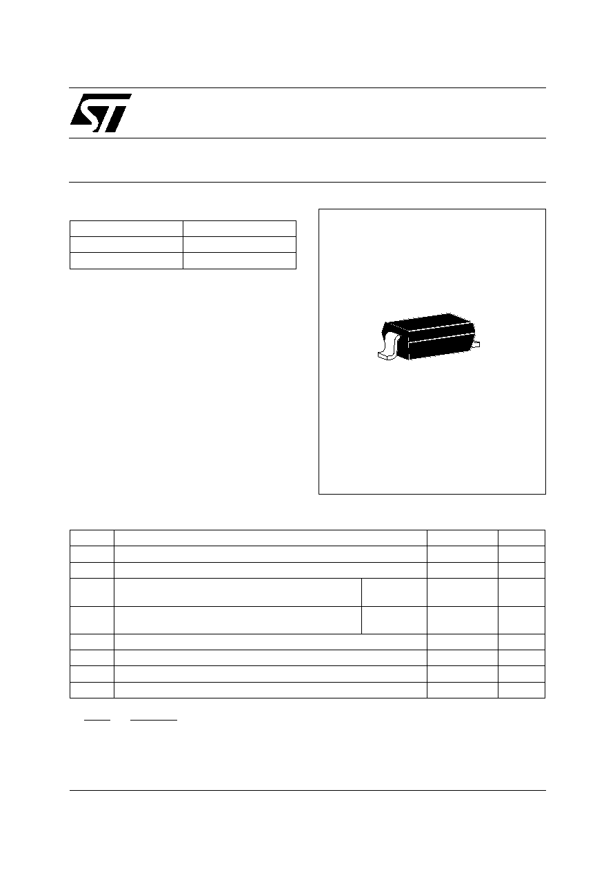
Packaged in SOD-123, this device is intended for
use in low voltage, high frequency inverters, free
wheeling and polarity protection applications. Due
to the small size of the package this device fits
GSM and PCMCIA requirements.
DESCRIPTION
SOD-123
Symbol
Parameter
Value
Unit
V
RRM
Repetitive peak reverse voltage
20
V
I
F(RMS)
RMS forward current
2
A
I
F(AV)
Average forward current
=0.5
Ta=25°C
0.5
A
I
FSM
Surge non repetitive forward current
tp=10ms
sinusoidal
5.5
A
dV/dt
Critical rate of rise of reverse voltage
10000
V/
µ
s
T
stg
Storage temperature range
- 65 to + 125
°C
Tj
Maximum operating junction temperature *
125
°
C
TL
Maximum temperature for soldering during 10s
260
°
C
ABSOLUTE RATINGS (limiting values)
* :
dPtot
dTj
Rth j
a
<
-
1
(
)
thermal runaway condition for a diode on its own heatsink
I
F(AV)
0.5 A
V
RRM
20 V
V
F
(max)
0.32 V
MAIN PRODUCT CHARACTERISTICS
STPS0520Z
2/5
Symbol
Parameter
Tests conditions
Value
Unit
STPS0520Z
typ.
max.
I
R
*
Reverse leakage current
Tj = 25°C
V
R
= 10 V
60
µ
A
Tj = 100°C
2.5
5
mA
Tj = 25°C
V
R
= V
RRM
150
µ
A
Tj = 100°C
4.3
8
mA
V
F
**
Forward voltage drop
Tj = 25°C
I
F
= 0.1 A
0.3
V
Tj = 100°C
0.18
0.22
Tj = 25°C
I
F
= 0.5 A
0.385
Tj=100°C
0.29
0.32
Pulse test :
* tp = 5 ms,
< 2%
** tp = 380
µ
s,
< 2%
To evaluate the maximum conduction losses use the following equation :
P = 0.23 x I
F(AV)
+ 0.18 x I
F
2
(RMS)
STATIC ELECTRICAL CHARACTERISTICS
Symbol
Parameter
Value
Unit
R
th (j-a)
Junction to ambient
430 (*)
210 (**)
°
C/W
(*) Mounted on epoxy board with recommended Pad Layout.
(**) Mounted on epoxy board with 50mm2 copper area.
THERMAL RESISTANCE
STPS0520Z
3/5
0.0
0.1
0.2
0.3
0.4
0.5
0.6
0.00
0.05
0.10
0.15
0.20
0.25
IF(av) (A)
PF(av)(W)
T
=tp/T
tp
= 0.05
= 0.1
= 0.2
= 0.5
= 1
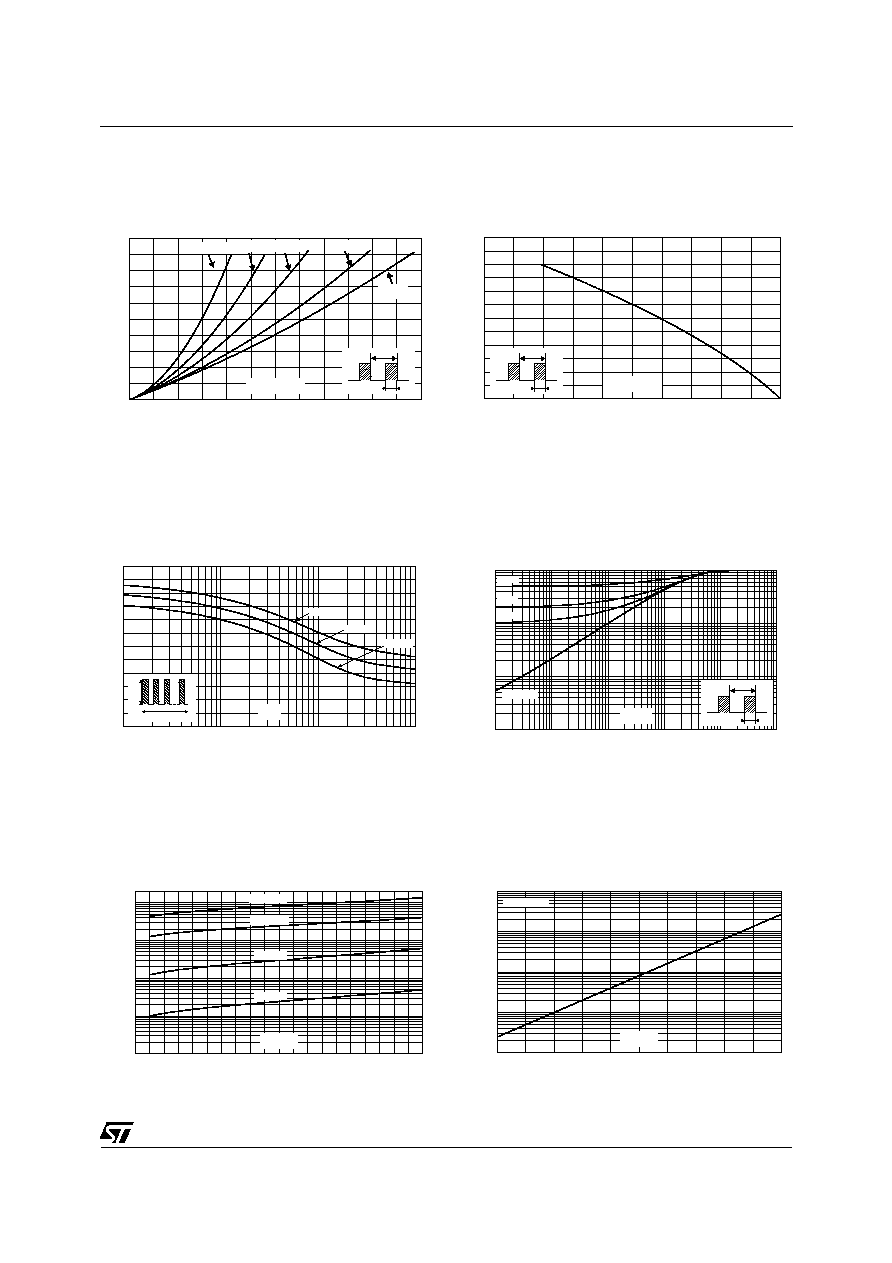
Fig. 1: Average forward power dissipation versus
average forward current
0
25
50
75
100
125
0.0
0.1
0.2
0.3
0.4
0.5
0.6
Tamb(°C)
IF(av)(A)
T
=tp/T
tp
Fig. 2: Average forward current versus ambient
temperature (
= 0.5)
1E-3
1E-2
1E-1
1E+0
0.0
0.5
1.0
1.5
2.0
2.5
3.0
t(s)
IM(A)
Ta=25°C
Ta=50°C
Ta=75°C
I
M
t
=0.5
Fig. 3: Non repetitive surge peak forward current
versus overload duration (maximum values).
1E-3
1E-2
1E-1
1E+0
1E+1
1E+2
1E-3
1E-2
1E-1
1E+0
tp(s)
Zth(j-a)/Rth(j-a)
= 0.5
= 0.2
= 0.1
Single pulse
T
=tp/T
tp
Fig. 4: Relative variation of thermal impedance
junction to ambient versus pulse duration (Epoxy
printed circuit board FR4 with recommended pad
layout).
0
2
4
6
8
10
12
14
16
18
20
1E-3
1E-2
1E-1
1E+0
1E+1
2E+1
VR(V)
IR(mA)
Tj=70°C
Tj=25°C
Tj=100°C
Tj=125°C
Fig. 5: Reverse leakage current versus reverse
voltage applied (typical values).
0
25
50
75
100
125
1E-1
1E+0
1E+1
1E+2
1E+3
Tj(°C)
IR[Tj] / IR[Tj=25°C]
VR=VRRM
Fig. 6: Relative variation of reverse leakage cur-
rent versus junction temperature (typical values).
STPS0520Z
4/5
1
2
5
10
20
10
20
50
100
200
VR(V)
C(pF)
F=1MHz
Tj=25°C
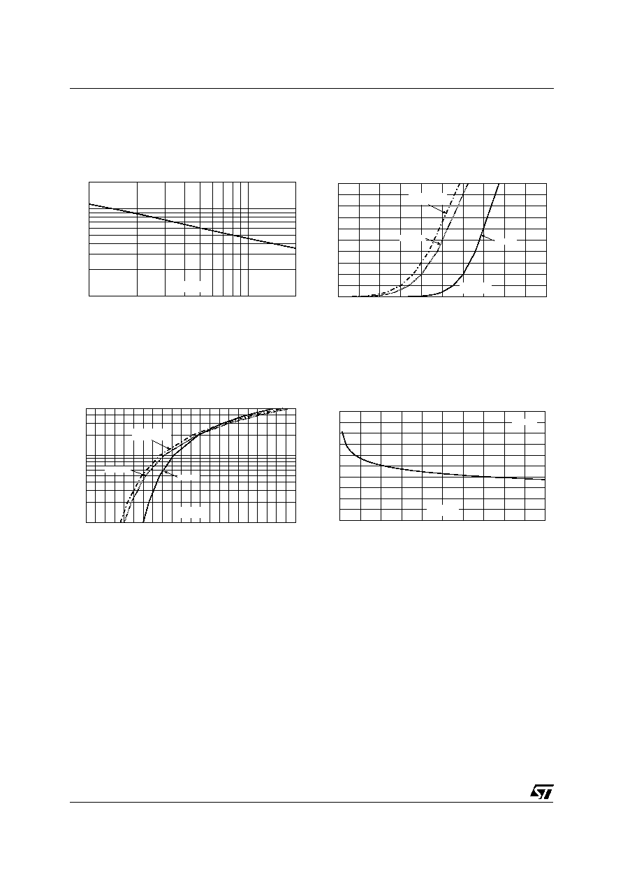
Fig. 7: Junction capacitance versus reverse volt-
age applied (typical values).
0.0
0.1
0.2
0.3
0.4
0.5
0.0
0.1
0.2
0.3
0.4
0.5
VFM(V)
IFM(A)
Tj=25°C
Tj=100°C
Tj=100°C
Typical values
Fig. 8-1: Forward voltage drop versus forward cur-
rent (maximum values, low level)
0.0 0.1 0.2 0.3 0.4 0.5 0.6 0.7 0.8 0.9 1.0 1.1
0.1
1.0
5.0
VFM(V)
IFM(A)
Tj=25°C
Tj=100°C
Tj=100°C
Typical values
Fig. 8-2: Forward voltage drop versus forward cur-
rent (maximum values, high level)
0
20
40
60
80
100
100
150
200
250
300
350
S(mm²)
Rth(j-a) (°C/W)
P=0.25W
Fig. 9: Variation of thermal resistance junction to
ambient versus copper surface under each lead
(Printed circuit board FR4, e(Cu) = 35µm).
STPS0520Z
5/5
Information furnished is believed to be accurate and reliable. However, STMicroelectronics assumes no responsibility for the consequences of
use of such information nor for any infringement of patents or other rights of third parties which may result from its use. No license is granted by
implication or otherwise under any patent or patent rights of STMicroelectronics. Specifications mentioned in this publication are subject to
change without notice. This publication supersedes and replaces all information previously supplied.
STMicroelectronics products are not authorized for use as critical components in life support devices or systems without express written ap-
proval of STMicroelectronics.
The ST logo is a registered trademark of STMicroelectronics
© 2002 STMicroelectronics - Printed in Italy - All rights reserved.
STMicroelectronics GROUP OF COMPANIES
Australia - Brazil - Canada - China - Finland - France - Germany
Hong Kong - India - Israel - Italy - Japan - Malaysia - Malta - Morocco - Singapore
Spain - Sweden - Switzerland - United Kingdom - United States.
http://www.st.com
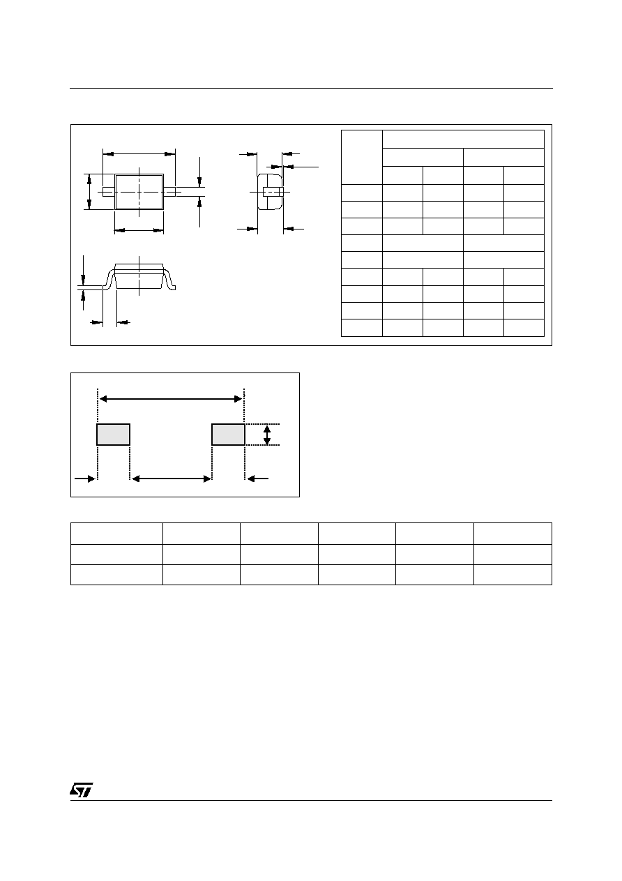
PACKAGE MECHANICAL DATA
SOD-123
H
b
D
E
A1
A2
A
G
c
REF.
DIMENSIONS
Millimeters
Inches
Min.
Max.
Min.
Max.
A
1.45
0.057
A1
0
0.1
0
0.004
A2
0.85
1.35
0.033
0.053
b
0.55 Typ.
0.022 Typ.
c
0.15 Typ.
0.039 Typ.
D
2.55
2.85
0.1
0.112
E
1.4
1.7
0.055
0.067
G
0.25
0.01
H
3.55
3.95
0.14
0.156
Type
Marking
Package
Weight
Base qty
Delivery mode
STPS0520Z
Z52
SOD-123
0.01g.
3000
Tape & reel
STPS0520Z10K
Z52
SOD-123
0.01 g
10000
Tape & reel
s
Epoxy meets UL94, V0.
s
Band indicates cathode.
MARKING
4.45
0.65
0.97
2.51
0.97
FOOTPRINT (in millimeters)