 | –≠–ª–µ–∫—Ç—Ä–æ–Ω–Ω—ã–π –∫–æ–º–ø–æ–Ω–µ–Ω—Ç: STPS120M | –°–∫–∞—á–∞—Ç—å:  PDF PDF  ZIP ZIP |

Æ
1/6
Table 1: Main Product Characteristics
I
F(AV)
1 A
V
RRM
20 V
T
j
(max)
150∞C
V
F
(max)
0.41 V
STPS120M
POWER SCHOTTKY RECTIFIER
REV. 3
Table 3: Absolute Ratings (limiting values)
Symbol
Parameter
Value
Unit
V
RRM
Repetitive peak reverse voltage
20
V
I
F(RMS)
RMS forward voltage
2
A
I
F(AV)
Average forward current
T
c
= 140∞C
= 0.5
1
A
I
FSM
Surge non repetitive forward current
tp = 8.3 ms sinusoidal
50
A
P
ARM
Repetitive peak avalanche power
tp = 1µs Tj = 25∞C
1400
W
T
stg
Storage temperature range
-65 to + 150
∞C
T
j
Maximum operating junction temperature *
150
∞C
dV/dt
Critical rate of rise of reverse voltage (rated V
R
, T
j
= 25∞C)
10000
V/µs
* :
thermal runaway condition for a diode on its own heatsink
dPtot
dTj
---------------
1
Rth j
a
≠
(
)
--------------------------
>
C
A
STmite
(DO216-AA)
September 2004
FEATURES AND BENEFITS
Very small conduction losses
Negligible switching losses
Extremely fast switching
Low forward voltage drop for higher efficiency
and extented battery life
Low thermal resistance
Avalanche capability specified
DESCRIPTION
Single Schottky rectifier suited for switch mode
power supplies and high frequency DC to DC
converters.
Packaged in STmite, this device is intended for
use in low voltage, high frequency inverters, free
wheeling and polarity protection applications. Due
to the small size of the package this device fits
battery powered equipment (cellular, notebook,
PDA's, printers) as well chargers and PCMCIA
cards.
Table 2: Order Code
Part Number
Marking
STPS120M
120
STPS120M
2/6
Table 4: Thermal Resistance
* Mounted with minimum recommended pad size, PC board FR4.
Table 5: Static Electrical Characteristics
Pulse test:
* tp = 380 µs,
< 2%
To evaluate the conduction losses use the following equation: P = 0.34 x IF(AV) + 0.07 IF
2
(RMS)
Symbol
Parameter
Value
Unit
R
th(j-c)
*
Junction to case
20
∞C/W
R
th(j-l)
*
Junction to ambient
250
∞C/W
Symbol
Parameter
Tests conditions
Min.
Typ
Max.
Unit
I
R
*
Reverse leakage current
T
j
= 25∞C
V
R
= V
RRM
1.3
3.9
µA
T
j
= 100∞C
275
850
T
j
= 25∞C
V
R
= 10V
0.6
2.0
T
j
= 100∞C
145
450
T
j
= 25∞C
V
R
= 5V
0.4
1.0
T
j
= 100∞C
105
300
V
F
*
Forward voltage drop
T
j
= 25∞C
I
F
= 1A
0.44
0.49
V
T
j
= 100∞C
0.36
0.41
T
j
= 25∞C
I
F
= 3A
0.48
0.54
T
j
= 100∞C
0.42
0.48
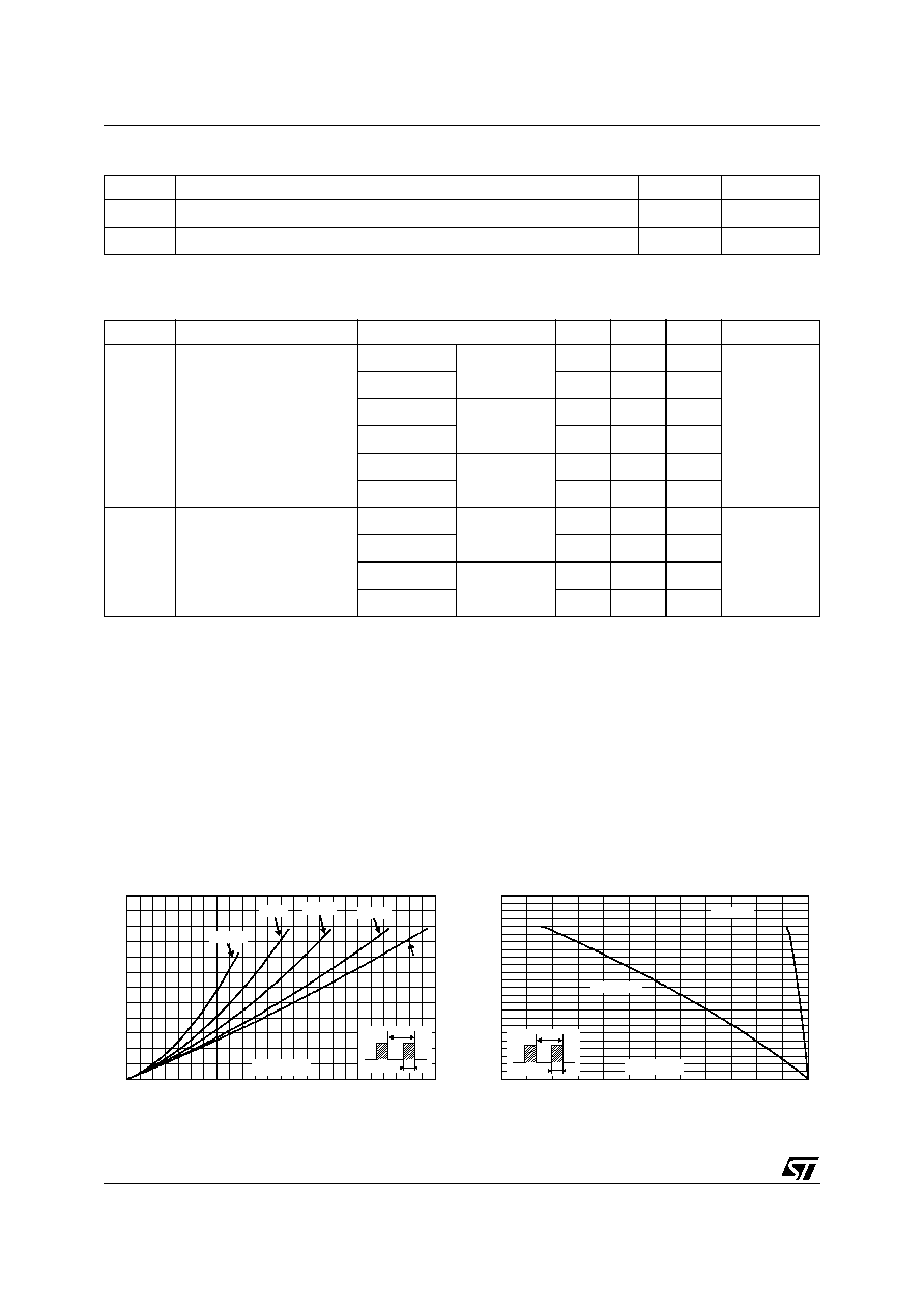
Figure 1: Conduction losses versus average
current
Figure 2: Average forward current versus
ambient temperature (
= 0.5)
P
(W)
F(AV)
= 1
0.0
0.1
0.2
0.3
0.4
0.5
0.6
0.0
0.1
0.2
0.3
0.4
0.5
0.6
0.7
0.8
0.9
1.0
1.1
1.2
= 0.05
= 0.2
= 0.5
= 0.1
T
=tp/T
tp
I
(A)
F(AV)
I
(A)
F(AV)
0.0
0.1
0.2
0.3
0.4
0.5
0.6
0.7
0.8
0.9
1.0
1.1
1.2
0
25
50
75
100
125
150
T
=tp/T
tp
T
(∞C)
amb
R
=R
th(j-a)
th(j-c)
R
=270∞C/W
th(j-a)

STPS120M
3/6
Figure 3: Normalized avalanche power
derating versus pulse duration
Figure 4: Normalized avalanche power
derating versus junction temperature
Figure 5: Non repetitive surge peak forward
current versus overload duration (maximum
values)
Figure 6: Relative variation of thermal
impedance junction to ambient versus pulse
duration
Figure 7: Reverse leakage current versus
reverse voltage applied (typical values)
Figure 8: Junction capacitance versus reverse
voltage applied (typical values)
0.001
0.01
0.1
0.01
1
0.1
10
100
1000
1
t (µs)
p
P
(t )
P
(1µs)
ARM p
ARM
0
0.2
0.4
0.6
0.8
1
1.2
25
50
75
100
125
150
T (∞C)
j
P
(t )
P
(25∞C)
ARM p
ARM
0
2
4
6
8
10
12
14
16
18
20
22
1.E-03
1.E-02
1.E-01
1.E+00
I
M
t
=0.5
I (A)
M
t(s)
T =25∞C
C
T =75∞C
C
T =125∞C
C
0.0
0.1
0.2
0.3
0.4
0.5
0.6
0.7
0.8
0.9
1.0
1.E-04
1.E-03
1.E-02
1.E-01
T
=tp/T
tp
= 0.5
= 0.2
= 0.1
Single pulse
Z
/R
th(j-c)
th(j-c)
t (s)
p
1.E-04
1.E-03
1.E-02
1.E-01
1.E+00
1.E+01
0
2
4
6
8
10
12
14
16
18
20
I (mA)
R
V (V)
R
T =125∞C
j
T =150∞C
j
T =100∞C
j
T =50∞C
j
T =25∞C
j
T =75∞C
j
10
100
1000
1
10
100
C(pF)
V (V)
R
F=1MHz
V
=30mV
T =25∞C
OSC
RMS
j

STPS120M
4/6
Figure 9: Forward voltage drop versus forward
current (low level)
Figure 10: Forward voltage drop versus
forward current (high level)
Figure 11: Thermal resistance junction to
ambient versus copper surface under tab
(epoxy printed board FR4, Cu = 35µm, typical
values)
0.0
0.2
0.4
0.6
0.8
1.0
1.2
1.4
1.6
1.8
2.0
0.0
0.1
0.2
0.3
0.4
0.5
0.6
I
(A)
FM
V
(V)
FM
T =25∞C
(maximum values)
j
T =100∞C
(maximum values)
j
T =100∞C
(typical values)
j
0.1
1.0
10.0
100.0
0.0
0.2
0.4
0.6
0.8
1.0
1.2
1.4
I
(A)
FM
V
(V)
FM
T =25∞C
(maximum values)
j
T =100∞C
(maximum values)
j
T =100∞C
(typical values)
j
R
(∞C/W)
th(j-a)
0
50
100
150
200
250
300
0.0
0.2
0.4
0.6
0.8
1.0
1.2
1.4
1.6
1.8
2.0
S(cm≤)

STPS120M
5/6
Figure 12: STmite Package Mechanical Data
Figure 13: Foot Print Dimensions (in millimeters)
C
L2
L
A1
R1
R
0∞ to 6∞
b
H
b2
D
L3
A
E
1.82
2.03
1.10
0.50
1.38
0.75
0.71
REF.
DIMENSIONS
Millimeters
Inches
Min.
Typ.
Max.
Min.
Typ.
Max.
A
0.85
1.00
1.15
0.033 0.039 0.045
A1
-0.05
0.05 -0.002
0.002
b
0.40
0.65
0.016
0.025
b2
0.70
1.00
0.027
0.039
c
0.10
0.25
0.004
0.010
D
1.75
1.90
2.05
0.069 0.007 0.081
E
1.75
1.90
2.05
0.069 0.007 0.081
H
3.60
3.75
3.90
0.142 0.148 0.154
L
0.50
0.63
0.80
0.020 0.025 0.031
L2
1.20
1.35
1.50
0.047 0.053 0.059
L3
0.50
ref
0.019
ref
R
0.07
0.003
R1
0.07
0.003
Table 6: Ordering Information
Ordering type
Marking
Package
Weight
Base qty
Delivery mode
STPS120M
120
STmite
15.5 mg
12000
Tape & reel
Table 7: Revision History
Date
Revision
Description of Changes
Jul-2003
2A
Last update.
13-Sep-2004
3
STmite package dimensions reference A1 change: from
blank (min) to -0.05mm and from 0.10 (max) to 0.05mm.