
1/4
STPS20100CT
Æ
August 2002 - Ed:2C
HIGH VOLTAGE POWER SCHOTTKY RECTIFIER
s
Negligible switching losses
s
Low forward voltage drop
s
Low capacitance
s
High reverse avalanche surge capability
FEATURES
High voltage dual Schottky rectifier suited for
switchmode power supplies and other power
converters. Packaged in TO-220AB, this device
is intended for use in medium voltage operation,
and particularly, in high frequency circuitries
where low switching losses and low noise are
required.
DESCRIPTION
A1
A2
K
TO-220AB
STP20100CT
A1
A2
K
I
F(AV)
2 x 10A
V
RRM
100V
V
F
(max)
0.7V
Tj (max)
175∞C
MAIN PRODUCT CHARACTERISTICS
Symbol
Parameter
Value
Unit
V
RRM
Repetitive peak reverse voltage
100
V
I
F(RMS)
RMS forward current
Per diode
30
A
I
F(AV)
Average forward current
= 0.5
Tc=110∞C
V
R
= 60V
Per diode
Per device
10
20
A
A
I
FSM
Surge non repetitive forward current
tp=10ms
sinusoidal
Per diode
200
A
I
RRM
Repetitive peak reverse current
tp=2
µ
s
F=1KHz
Per diode
1
A
I
RSM
Non repetitive peak reverse current
tp=100
µ
s
Per diode
1
A
Tstg
Storage temperature range
- 65 to + 175
∞
C
Tj
Maximum junction temperature (*)
175
∞C
dV/dt
Critical rate of rise of reverse voltage
1000
V/
µ
s
* :
dPtot
dTj
Rth j
a
<
-
1
(
)
thermal runaway condition for a diode on its own heatsink
ABSOLUTE MAXIMUM RATINGS
STPS20100CT
2/4
Symbol
Parameter
Value
Unit
Rth (j-c)
Junction to case
Per diode
1.6
∞C/W
Total
0.9
Rth (c)
Coupling
0.15
∞C/W
When the diodes 1 and 2 are used simultaneously :
Tj-Tc(diode 1)=P(diode1) x Rth(j-c)(Per diode) + P(diode 2) x Rth(c)
THERMAL RESISTANCES
Symbol
Parameter
Test Conditions
Min.
Typ.
Max.
Unit
I
R
*
Reverse leakage current
V
R
= V
RRM
Tj = 25∞C
150
µA
Tj = 125∞C
100
mA
V
F
**
Forward voltage drop
IF = 20A
Tj = 125∞C
0.85
V
IF = 10A
Tj = 125∞C
0.60
0.70
IF = 20A
Tj = 25∞C
0.95
Pulse test : * tp = 5 ms, duty cycle < 2 %
** tp = 380
µ
s, duty cycle < 2 %
To evaluate the conduction losses use the following equation :
P = 0.55 x I
F(AV)
+ 0.015 x I
F
2
(RMS)
ELECTRICAL CHARACTERISTICS (Per diode)
STATIC CHARACTERISTICS
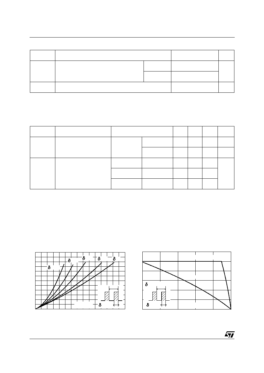
0
1
2
3
4
5
6
7
8
9 10 11 12 13 14 15
0
1
2
3
4
5
6
7
8
9
10
11
12
=0.05
=0.1
=0.2
=0.5
T
=tp/T
tp
IF(av)(A)
PF(av)(W)
=1
Fig. 1 : Average forward power dissipation versus
average forward current. (Per diode)
0
25
50
75
100
125
0
2
4
6
8
10
12
T
=tp/T
tp
=0.5
F(av)(A)
I
o
Tamb( C)
Rth(j-a)=15
C/W
o
Rth(j-a)=Rth(j-c)
Fig.
2
:
Average
current
versus
ambient
temperature. (duty cycle : 0.5) (Per diode)

STPS20100CT
3/4
0.001
0.01
0.1
1
0
20
40
60
80
100
120
140
160
180
IM
t
=0.5
t(s)
IM(A)
Tc=25 C
o
Tc=50 C
o
Tc=110
C
o
Fig. 3 : Non repetitive surge peak forward current
versus overload duration.
(Maximum values) (Per diode)
Fig. 4 : Relative variation of thermal transient
impedance junction to case versus pulse duration.
0
10
20
30
40
50
60
70
80
90 100
0.001
0.010
0.100
1.000
10.000
50.000
Tj=125
C
o
VR(V)
IR(mA)
Tj=75
C
o
Tj=50
C
o
Tj=100
C
o
Fig. 5 : Reverse leakage current versus reverse
voltage applied. (Typical values) (Per diode)
1
10
100
100
1000
2000
VR(V)
Tj=125
C
o
C(pF)
F= 1MH z
Fig. 6 : Junction capacitance versus reverse
voltage applied. (Typical values) (Per diode)
0.1
1
10
100
0.0
0.2
0.4
0.6
0.8
1.0
1.2
1.4
I FM(A)
VFM(V)
Tj=125
C
o
Fig. 7 : Forward voltage drop versus forward
current. (Maximum values) (Per diode)
STPS20100CT
4/4
Information furnished is believed to be accurate and reliable. However, STMicroelectronics assumes no responsibility for the consequences of
use of such information nor for any infringement of patents or other rights of third parties which may result from its use. No license is granted by
implication or otherwise under any patent or patent rights of STMicroelectronics. Specifications mentioned in this publication are subject to
change without notice. This publication supersedes and replaces all information previously supplied.
STMicroelectronics products are not authorized for use as critical components in life support devices or systems without express written ap-
proval of STMicroelectronics.
The ST logo is a registered trademark of STMicroelectronics
© 2002 STMicroelectronics - Printed in Italy - All rights reserved.
STMicroelectronics GROUP OF COMPANIES
Australia - Brazil - Canada - China - Finland - France - Germany
Hong Kong - India - Israel - Italy - Japan - Malaysia - Malta - Morocco - Singapore
Spain - Sweden - Switzerland - United Kingdom - United States.
http://www.st.com
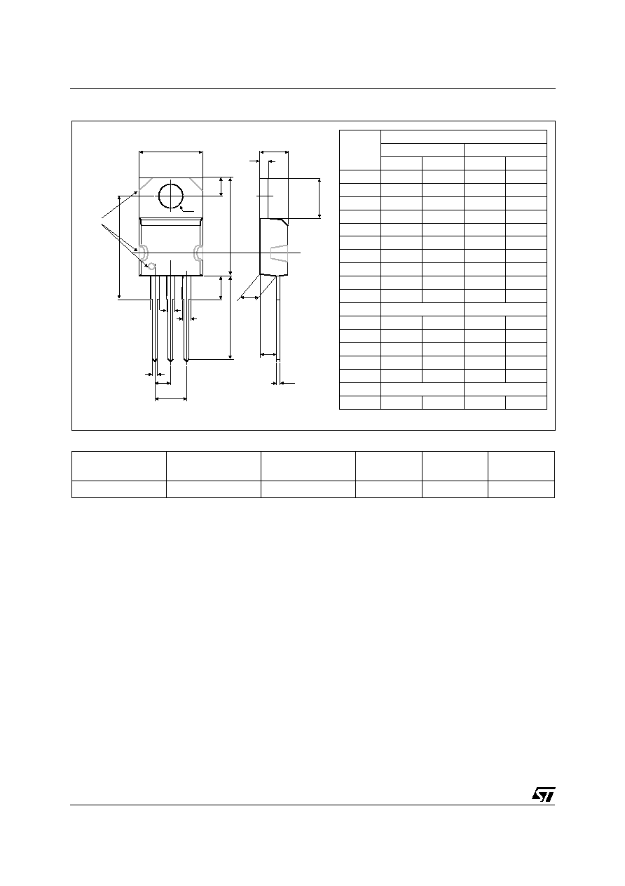
PACKAGE MECHANICAL DATA
TO-220AB (JEDEC outline)
M
H2
L2
A
C
L4
F1(x2)
D
F2
F
G
L9
L6
L7
L5
G1
E
Dia
OPTIONAL
REF.
DIMENSIONS
Millimeters
Inches
Min.
Max.
Min.
Max.
A
4.30
4.60
0.169
0.181
C
1.22
1.32
0.048
0.052
D
2.40
2.72
0.094
0.107
E
0.33
0.70
0.013
0.028
F
0.61
0.93
0.024
0.037
F1
1.14
1.70
0.045
0.067
F2
1.14
1.70
0.045
0.067
G
4.95
5.15
0.195
0.202
G1
2.40
2.70
0.094
0.106
H2
10.00
10.40
0.394
0.409
L2
16.00 Typ.
0.630 Typ.
L4
13.00
14.00
0.512
0.551
L5
2.65
2.95
0.104
0.116
L6
14.80
15.75
0.583
0.620
L7
6.20
6.60
0.244
0.260
L9
3.40
3.94
0.134
0.155
M
2.60 Typ.
0.102 Typ.
Dia.
3.75
3.89
0.148
0.153
Ordering type
Marking
Package
Weight
Base qty
Delivery
mode
STPS20100CT
STPS20100CT
TO-220AB
2.23g
50
Tube
s
Cooling method : by conduction (C)
s
Recommended torque value : 0.55N.m.
s
Maximum torque value : 0.7N.m.
s
Epoxy meets UL94,V0