
1/9
STPS20L45CF/CW/CT/CFP/CG
July 2003 - Ed: 3C
LOW DROP POWER SCHOTTKY RECTIFIER
Æ
Dual center tap Schottky rectifiers designed for
high frequency switched mode power supplies and
DC to DC converters.
These devices are intended for use in low voltage,
high
frequency
inverters,
free-wheeling
and
polarity protection applications.
DESCRIPTION
s
LOW FORWARD VOLTAGE DROP MEANING
VERY SMALL CONDUCTION LOSSES
s
LOW SWITCHING LOSSES ALLOWING HIGH
FREQUENCY OPERATION
s
INSULATED
PACKAGE:
ISOWATT220AB,
TO-220FPAB
Insulating voltage = 2000V DC
Capacitance = 12pF
s
AVALANCHE CAPABILITY SPECIFIED
FEATURES AND BENEFITS
Symbol
Parameter
Value
Unit
V
RRM
Repetitive peak reverse voltage
45
V
I
F(RMS)
RMS forward current
30
A
I
F(AV)
Average forward
current
TO-220AB / D
2
PAK
TO-247
Tc = 135∞C
= 0.5
Per diode
Per device
10
20
A
ISOWATT220AB
TO-220FPAB
Tc = 115∞C
= 0.5
Per diode
Per device
10
20
A
I
FSM
Surge non repetitive forward current
tp = 10 ms Sinusoidal
180
A
I
RRM
Peak repetitive reverse current
tp=2 µs square F=1kHz
1
A
I
RSM
Non repetitive peak reverse current
tp = 100 µs square
2
A
P
ARM
Repetitive peak avalanche power
tp = 1µs
Tj = 25∞C
4000
W
T
stg
Storage temperature range
- 65 to + 150
∞C
Tj
Maximum operating junction temperature *
150
∞C
dV/dt
Critical rate of rise of reverse voltage
10000
V/µs
ABSOLUTE RATINGS (limiting values, per diode)
I
F(AV)
2 x 10 A
V
RRM
45 V
Tj (max)
150∞C
V
F
(max)
0.5 V
MAJOR PRODUCTS CHARACTERISTICS
A1
K
A2
A1
K
A2
ISOWATT220AB
STPS20L45CF
TO-247
STPS20L45CW
K
A1
A2
TO-220AB
STPS20L45CT
* :
dPtot
dTj
Rth j
a
<
-
1
(
)
thermal runaway condition for a diode on its own heatsink
A1
K
A2
A1
A2
K
TO-220FPAB
STPS20L45CFP
K
A1
A2
D
2
PAK
STPS20L45CG
STPS20L45CF/CW/CT/CFP/CG
2/9
Symbol
Parameter
Tests Conditions
Min.
Typ.
Max.
Unit
I
R
*
Reverse leakage
current
Tj = 25∞C
V
R
= V
RRM
0.2
mA
Tj = 125∞C
65
130
mA
V
F
*
Forward voltage drop
Tj = 25
∞
C
I
F
= 10 A
0.55
V
Tj = 125∞C
I
F
= 10 A
0.44
0.5
Tj = 25
∞
C
I
F
= 20 A
0.73
Tj = 125∞C
I
F
= 20 A
0.62
0.72
Pulse test : * tp = 380 µs,
< 2%
To evaluate the conduction losses use the following equation :
P = 0.28 x I
F(AV)
+ 0.022 I
F
2
(RMS)
STATIC ELECTRICAL CHARACTERISTICS (per diode)
Symbol
Parameter
Value
Unit
R
th(j-c)
Junction to case
ISOWATT220AB
TO-220FPAB
Per diode
Total
Coupling
4.5
3.5
2.5
∞C/W
R
th(j-c)
Junction to case
TO-247
Per diode
Total
Coupling
2.2
1.20
0.3
∞C/W
R
th(j-c)
Junction to case
TO-220AB
D
2
PAK
Per diode
Total
Coupling
2.2
1.3
0.3
∞C/W
THERMAL RESISTANCES
0
2
4
6
8
10
12
14
0
1
2
3
4
5
6
7
8
IF(av) (A)
PF(av)(W)
= 0.2
= 0.5
= 1
= 0.05
= 0.1
T
=tp/T
tp
Fig. 1: Average forward power dissipation versus
average forward current (per diode).
0
25
50
75
100
125
150
0
1
2
3
4
5
6
7
8
9
10
11
12
IF(av)(A)
Rth(j-a)=15∞C/W
Rth(j-a)=Rth(j-c)
TO-220AB/TO-247
ISOWATT220AB
T
=tp/T
tp
Tamb(∞C)
Fig. 2: Average forward current versus ambient
temperature(
= 0.5, per diode).
When the diodes 1 and 2 are used simultaneously :
Tj(diode 1) = P(diode1) x R
th(j-c)
(Per diode) + P(diode 2) x R
th(c)

STPS20L45CF/CW/CT/CFP/CG
3/9
1E-3
1E-2
1E-1
1E+0
0.0
0.2
0.4
0.6
0.8
1.0
tp(s)
Zth(j-c)/Rth(j-c)
= 0.1
= 0.2
= 0.5
Single pulse
T
=tp/T
tp
Fig. 6-1: Relative variation of thermal impedance
junction to case versus pulse duration (TO-220AB,
TO-247, D
2
PAK).
1E-3
1E-2
1E-1
1E+0
1E+1
0.0
0.2
0.4
0.6
0.8
1.0
tp(s)
Zth(j-c)/Rth(j-c)
T
=tp/T
tp
= 0.1
= 0.2
= 0.5
Single pulse
Fig. 6-2: Relative variation of thermal impedance
junction
to
case
versus
pulse
duration
(ISOWATT220AB, TO-220FPAB).
1E-3
1E-2
1E-1
1E+0
0
10
20
30
40
50
60
70
80
90
100
IM(A)
Tc=25∞C
Tc=100∞C
Tc=50∞C
I
M
t
=0.5
t(s)
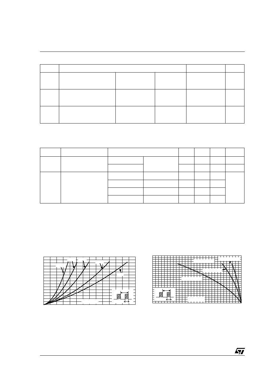
Fig. 5-2: Non repetitive surge peak forward
current versus overload duration (maximum
values,
per
diode,
ISOWATT220AB,
TO-220FPAB).
1E-3
1E-2
1E-1
1E+0
0
20
40
60
80
100
120
140
IM(A)
Tc=25∞C
Tc=125∞C
Tc=75∞C
t(s)
I
M
t
=0.5
Fig. 5-1: Non repetitive surge peak forward
current versus overload duration (maximum
values,
per
diode,
TO-220AB,
TO-247,
D
2
PAK).
0
0.2
0.4
0.6
0.8
1
1.2
0
25
50
75
100
125
150
T (∞C)
j
P
(t )
P
(25∞C)
ARM p
ARM
Fig. 4: Normalized avalanche power derating
versus junction temperature.
0.001
0.01
0.1
0.01
1
0.1
10
100
1000
1
t (µs)
p
P
(t )
P
(1µs)
ARM p
ARM
Fig. 3: Normalized avalanche power derating
versus pulse duration.

STPS20L45CF/CW/CT/CFP/CG
4/9
0.0
0.2
0.4
0.6
0.8
1.0
1.2
1.4
1.6
0.1
1.0
10.0
100.0
IFM(A)
Tj=75∞C
Tj=25∞C
Tj=125∞C
Typical values
Tj=150∞C
VFM(V)
Fig. 9: Forward voltage drop versus forward
current (maximum values) (per diode).
0
4
8
12
16
20
24
28
32
36
40
0
10
20
30
40
50
60
70
80
S(Cu) (cm≤)
Rth(j-a) (∞C/W)
Fig. 10: Thermal resistance junction to ambient
versus copper surface under tab (Epoxy printed cir-
cuit board FR4, copper thickness: 35µm) (D
2
PAK).
0
5
10
15
20
25
30
35
40
45
1E-3
1E-2
1E-1
1E+0
1E+1
1E+2
2E+2
VR(V)
IR(mA)
Tj=75∞C
Tj=25∞C
Tj=125∞C
Tj=150∞C
Fig. 7: Reverse leakage current versus reverse
voltage applied (typical values, per diode).
1
2
5
10
20
50
100
1000
2000
VR(V)
C(pF)
F=1MHz
Tj=25∞C
Fig. 8: Junction capacitance versus reverse
voltage applied (typical values, per diode).

STPS20L40CF/CW/CT
5/9
s
Cooling method : C
s
Recommended torque value : 0.55 m.N
s
Maximum torque value : 0.70 m.N
PACKAGE MECHANICAL DATA
ISOWATT220AB
REF.
DIMENSIONS
Millimeters
Inches
Min.
Max.
Min.
Max.
A
4.40
4.60
0.173
0.181
B
2.50
2.70
0.098
0.106
D
2.50
2.75
0.098
0.108
E
0.40
0.70
0.016
0.028
F
0.75
1.00
0.030
0.039
F1
1.15
1.70
0.045
0.067
F2
1.15
1.70
0.045
0.067
G
4.95
5.20
0.195
0.205
G1
2.40
2.70
0.094
0.106
H
10.00
10.40
0.394
0.409
L2
16.00 typ.
0.630 typ.
L3
28.60
30.60
1.125
1.205
L4
9.80
10.60
0.386
0.417
L6
15.90
16.40
0.626
0.646
L7
9.00
9.30
0.354
0.366
Diam
3.00
3.20
0.118
0.126