 | –≠–ª–µ–∫—Ç—Ä–æ–Ω–Ω—ã–π –∫–æ–º–ø–æ–Ω–µ–Ω—Ç: STPS340S | –°–∫–∞—á–∞—Ç—å:  PDF PDF  ZIP ZIP |
STPS340U/S/B
June 1999 - Ed: 6B
POWER SCHOTTKY RECTIFIER
Æ
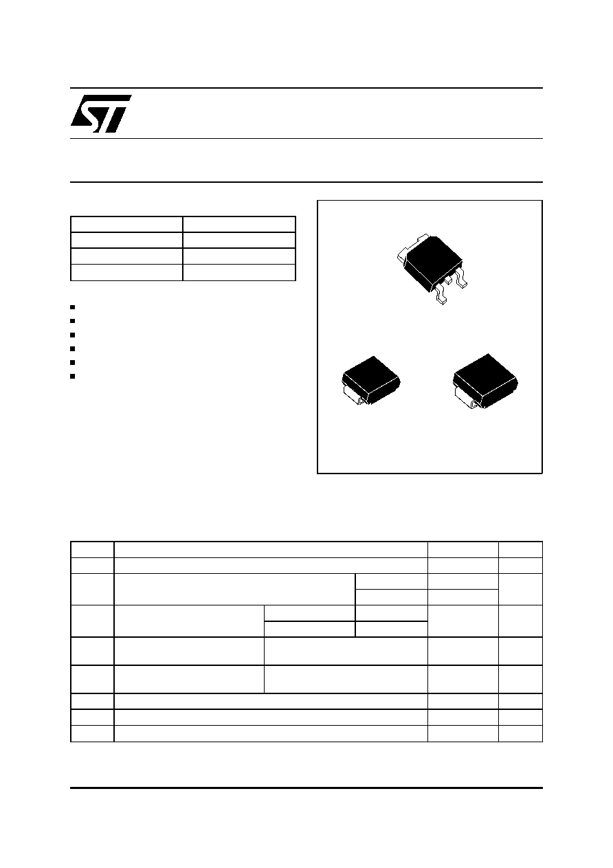
Single chip Schottky rectifier suited for Switch
Mode Power Supplies and high frequency DC to
DC converters.
Packaged in SMB, SMC and DPAK this device is
intended for use in low and medium voltage
operation, high frequency inverters, free wheeling
and polarity protection applications where low
switching losses are required.
DESCRIPTION
SMB
(JEDEC DO-214AA)
STPS340U
VERY SMALL CONDUCTION LOSSES
NEGLIGIBLE SWITCHING LOSSES
LOW FORWARD VOLTAGE DROP
LOW THERMAL RESISTANCE
EXTREMELY FAST SWITCHING
SURFACE MOUNTED DEVICE
Symbol
Parameter
Value
Unit
V
RRM
Repetitive peak reverse voltage
40
V
I
F(RMS)
RMS forward current
DPAK
6
A
SMB / SMC
10
I
F(AV)
Average forward current
T
c
= 135∞C
= 0.5
DPAK
3
A
T
L
= 105
∞
C
= 0.5
SMB / SMC
I
FSM
Surge non repetitive forward
current
tp = 10 ms Sinusoidal
75
A
I
RRM
Repetitive peak reverse
current
tp = 2
µ
s F = 1kHz square
1
A
Tstg
Storage temperature range
- 65 to + 150
∞
C
Tj
Maximum operating junction temperature
+ 150
∞
C
dV/dt
Critical rate of rise of reverse voltage
10000
V/
µ
s
ABSOLUTE RATINGS (limiting values)
SMC
(JEDEC DO-214AB)
STPS340S
K
A
NC
DPAK
STPS340B
I
F(AV)
3 A
V
RRM
40 V
Tj (max)
150 ∞C
V
F
(max)
0.57 V
MAIN PRODUCT CHARACTERISTICS
1/7

Symbol
Tests Conditions
Tests Conditions
Min.
Typ.
Max.
Unit
I
R
*
Reverse leakage current
Tj = 25
∞
C
V
R
= V
RRM
20
µ
A
Tj = 125
∞
C
V
R
= V
RRM
2
10
mA
V
F
*
Forward voltage drop
Tj = 25
∞
C
I
F
= 3 A
0.63
V
Tj = 25
∞
C
I
F
= 6 A
0.84
Tj = 125
∞
C
I
F
= 3 A
0.52
0.57
Tj = 125
∞
C
I
F
= 6 A
0.63
0.72
STATIC ELECTRICAL CHARACTERISTICS
Pulse test : * tp = 380
µ
s,
< 2 %
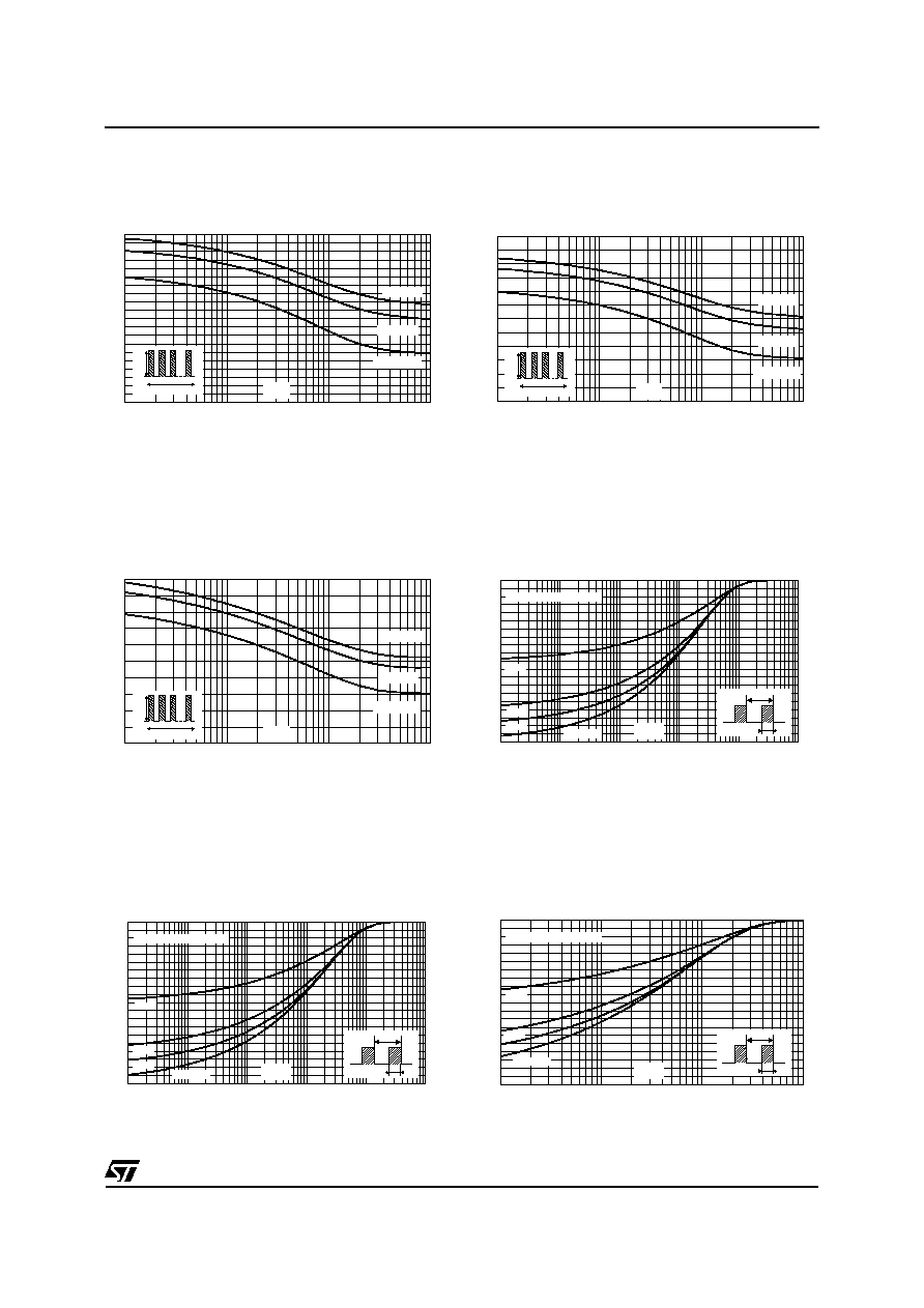
To evaluate the maximum conduction losses use the following equation :
P = 0.42 x I
F(AV)
+ 0.050 I
F
2
(RMS)
0.0
0.5
1.0
1.5
2.0
2.5
3.0
3.5
4.0
0.0
0.5
1.0
1.5
2.0
2.5
IF(av) (A)
PF(av)(W)
T
=tp/T
tp
= 1
= 0.5
= 0.2
= 0.1
= 0.05
Fig. 1: Average forward power dissipation versus
average forward current.
0
25
50
75
100
125
150
0.0
0.5
1.0
1.5
2.0
2.5
3.0
3.5
Tamb(∞C)
IF(av)(A)
Rth(j-a)=65∞C/W
Rth(j-a)=Rth(j-l)
(SMB/SMC)
Rth(j-a)=Rth(j-c)
(DPAK)
T
=tp/T
tp
Fig. 2: Average current versus ambient
temperature
(
=0.5)
.
Symbol
Parameter
Value
Unit
R
th (j-l)
Junction to leads
SMC
20
∞
C/W
SMB
25
R
th (j-c)
Junction to case
DPAK
5.5
∞C/W
THERMAL RESISTANCES
STPS340U/S/B
2/7
1E-3
1E-2
1E-1
1E+0
0
1
2
3
4
5
6
7
8
9
10
t(s)
IM(A)
Ta=25∞C
Ta=50∞C
Ta=100∞C
I
M
t
=0.5
Fig. 3-1: Non repetitive surge peak forward current
versus overload duration (SMB)(Maximum values).
1.0E-2
1.0E-1
1.0E+0
1.0E+1
1.0E+2
1.0E+3
0.0
0.1
0.2
0.3
0.4
0.5
0.6
0.7
0.8
0.9
1.0
tp(s)
Zth(j-a)/Rth(j-a)
Printed circuit board (e=35µm)
T
=tp/T
tp
Single pulse
= 0.1
= 0.2
= 0.5
Fig. 4-1: Relative variation of thermal transient
impedance junction to lead versus pulse duration
(SMB).
1E-3
1E-2
1E-1
1E+0
0
2
4
6
8
10
12
Ta=25∞C
Ta=50∞C
Ta=100∞C
t(s)
IM(A)
I
M
t
=0.5
Fig. 3-2: Non repetitive surge peak forward current
versus overload duration (SMC) (Maximum values).
1E-3
1E-2
1E-1
1E+0
0
10
20
30
40
50
Tc=25∞C
Tc=50∞C
Tc=100∞C
t(s)
IM(A)
I
M
t
=0.5
Fig. 3-3: Non repetitive surge peak forward current
versus overload duration (DPAK) (Maximum
values).
1.0E-2
1.0E-1
1.0E+0
1.0E+1
1.0E+2
1.0E+3
0.0
0.1
0.2
0.3
0.4
0.5
0.6
0.7
0.8
0.9
1.0
tp(s)
Zth(j-a)/Rth(j-a)
T
=tp/T
tp
Printed circuit board (e=35µm)
Single pulse
= 0.1
= 0.2
= 0.5
Fig. 4-2: Relative variation of thermal transient
impedance junction to lead versus pulse duration
(SMC).
1E-3
1E-2
1E-1
1E+0
0.0
0.1
0.2
0.3
0.4
0.5
0.6
0.7
0.8
0.9
1.0
tp(s)
Zth(j-a)/Rth(j-a)
T
=tp/T
tp
Printed circuit board (e=35µm)
Single pulse
= 0.1
= 0.2
= 0.5
Fig. 4-3: Relative variation of thermal transient
impedance junction to lead versus pulse
duration(DPAK).
STPS340U/S/B
3/7

1
2
5
10
20
50
10
20
50
100
200
500
VR(V)
C(pF)
F=1MHz
Tj=25∞C
Fig. 6: Junction capacitance versus reverse
voltage applied (Typical values).
0.0 0.1 0.2 0.3 0.4 0.5 0.6 0.7 0.8 0.9 1.0
0.01
0.10
1.00
10.00
IFM(A)
Typical values
Tj=150∞C
Tj=125∞C
VFM(V)
Fig. 7: Forward voltage drop versus forward
current (Maximum values).
0
5
10
15
20
25
30
35
40
1E-5
1E-4
1E-3
1E-2
VR(V)
IR(A)
Tj=125∞C
Tj=100∞C
Tj=75∞C
Tj=150∞C
Fig. 5: Reverse leakage current versus reverse
voltage applied (Typical values).
0
1
2
3
4
5
0
20
40
60
80
100
120
S(Cu) (cm≤)
Rth(j-a) (∞C/W)
Fig. 8-1: Thermal resistance junction to ambient
versus copper surface under each lead (Epoxy printed
circuit board FR4, copper thickness: 35
µ
m) (SMB).
0
1
2
3
4
5
0
20
40
60
80
100
Rth(j-a) (∞C/W)
S(Cu) (cm≤)
Fig. 8-2: Thermal resistance junction to ambient
versus copper surface under each lead (Epoxy printed
circuit board FR4, copper thickness: 35
µ
m) (SMC).
0
2
4
6
8
10
12
14
16
18
20
0
20
40
60
80
100
Rth(j-a) (∞C/W)
S(Cu) (cm≤)
Fig. 8-3: Thermal resistance junction to ambient
versus copper surface under each lead (Epoxy printed
circuit board FR4, copper thickness: 35
µ
m) (DPAK).
STPS340U/S/B
4/7
PACKAGE MECHANICAL DATA
DPAK
REF.
DIMENSIONS
Millimeters
Inches
Min.
Max
Min.
Max.
A
2.20
2.40
0.086
0.094
A1
0.90
1.10
0.035
0.043
A2
0.03
0.23
0.001
0.009
B
0.64
0.90
0.025
0.035
B2
5.20
5.40
0.204
0.212
C
0.45
0.60
0.017
0.023
C2
0.48
0.60
0.018
0.023
D
6.00
6.20
0.236
0.244
E
6.40
6.60
0.251
0.259
G
4.40
4.60
0.173
0.181
H
9.35
10.10
0.368
0.397
L2
0.80 typ.
0.031 typ.
L4
0.60
1.00
0.023
0.039
V2
0∞
8∞
0∞
8∞
6.7
6.7
3
3
1.6
1.6
2.3
2.3
FOOTPRINT DIMENSIONS (in millimeters)
STPS340U/S/B
5/7