1/7
PRODUCT PREVIEW
July 2004
This is preliminary information on a new product now in development. Details are subject to change without notice
STS12NH3LL
N-CHANNEL 30 V - 0.008
- 12 A SO-8
ULTRA LOW GATE CHARGE STripFETTM MOSFET
Table 1: General Features
s
TYPICAL R
DS
(on) = 0.008
@ 10V
s
OPTIMAL R
DS
(on) x Qg TRADE-OFF @ 4.5 V
s
SWITCHING LOSSES REDUCED
s
LOW THRESHOLD DEVICE
s
LOW INPUT CAPACITANCE
DESCRIPTION
The STS12NH3LL is based on the latest genera-
tion of ST's proprietary "STripFETTM" technology.
An innovative layout enables the device to also ex-
hibit extremely low gate charge for the most de-
manding requirements as high-side switch in high-
frequency DC-DC converters. It's therefore ideal
for high-density converters in Telecom and Com-
puter applications.
APPLICATIONS
s
HIGH FREQUENCY DC-DC CONVERTERS
FOR COMPUTER AND TELECOM
Table 2: Order Codes
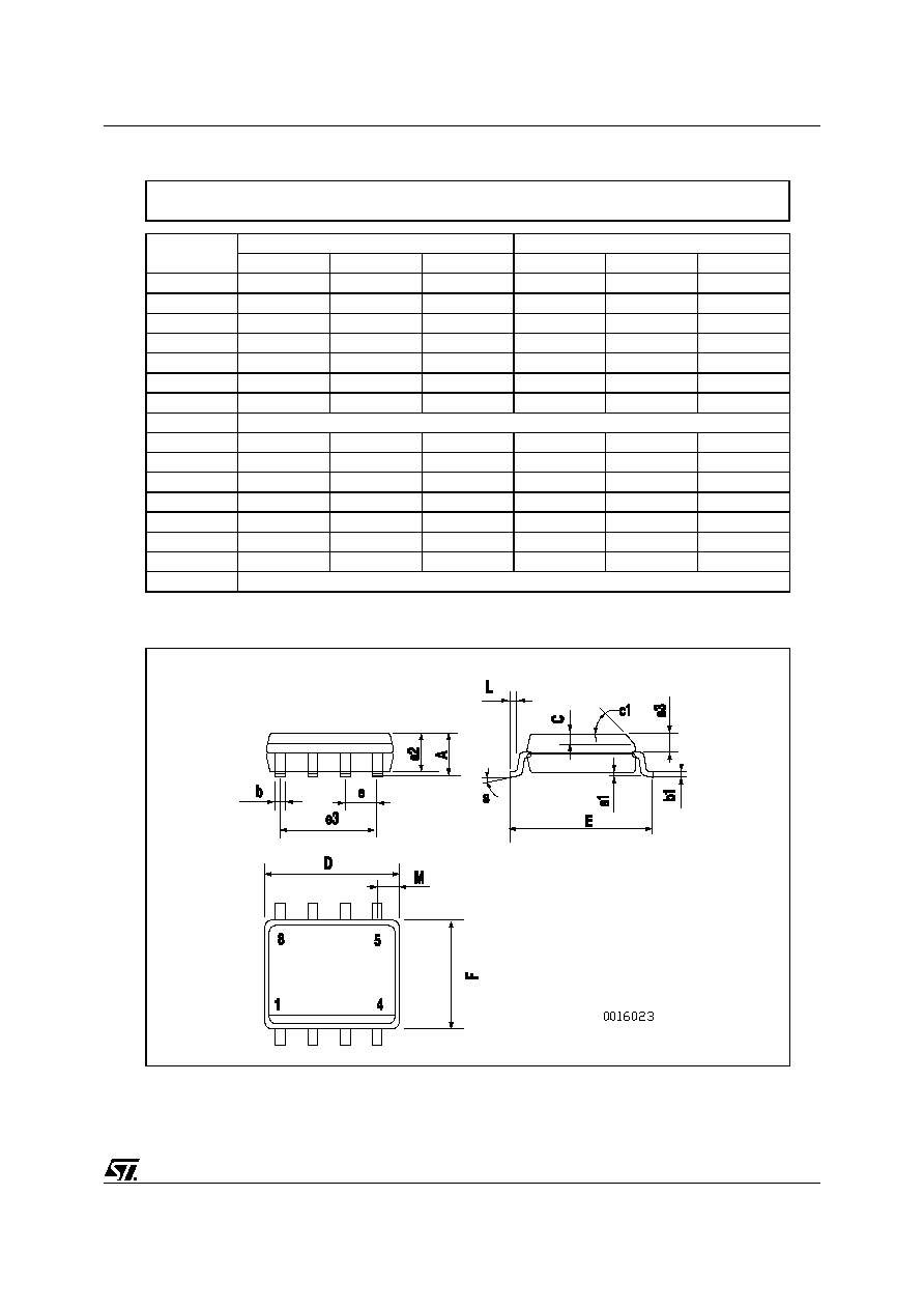
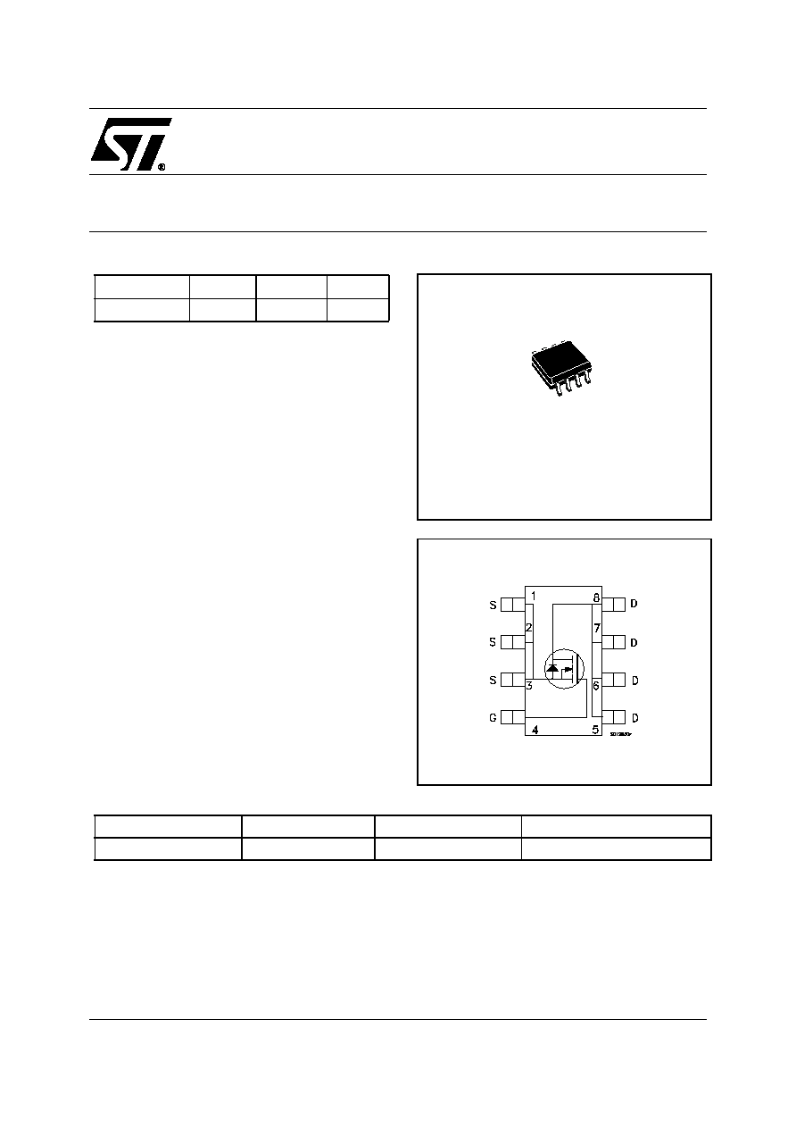
Figure 1: Package
Figure 2: Internal Schematic Diagram
TYPE
V
DSS
R
DS(on)
I
D
STS12NH3LL
30 V
< 0.0105
12 A
SO-8
Part Number
Marking
Package
Packaging
STS12NH3LL
S12NH3LL
SO-8
TAPE & REEL
Rev. 3

STS12NH3LL
2/7
Table 3: Absolute Maximum ratings
(
) Pulse width limited by safe operating area
Table 4: Thermal Data
(
#
) When Mounted on 1 inch� FR-4 board, 2 oz Cu (t
10 sec.)
ELECTRICAL CHARACTERISTICS (T
CASE
=25�C UNLESS OTHERWISE SPECIFIED)
Table 5: On /Off
Table 6: Dynamic
Symbol
Parameter
Value
Unit
V
DS
Drain-source Voltage (V
GS
= 0)
30
V
V
DGR
Drain-gate Voltage (R
GS
= 20 k
)
30
V
V
GS
Gate-source Voltage
� 16
V
I
D
Drain Current (continuous) at T
C
= 25�C
12
A
I
D
Drain Current (continuous) at T
C
= 100�C
7.5
A
I
DM
( )
Drain Current (pulsed)
48
A
P
tot
Total Dissipation at T
C
= 25�C
2.5
W
T
stg
Storage Temperature
� 55 to 150
�C
T
j
Max. Operating Junction Temperature
Rthj-amb (#)
Thermal Resistance Junction-ambient
50
�C/W
Symbol
Parameter
Test Conditions
Min.
Typ.
Max.
Unit
V
(BR)DSS
Drain-source Breakdown
Voltage
I
D
= 250 �A, V
GS
= 0
30
V
I
DSS
Zero Gate Voltage
Drain Current (V
GS
= 0)
V
DS
= Max Rating
V
DS
= Max Rating, T
C
= 125�C
1
10
�A
�A
I
GSS
Gate-body Leakage
Current (V
DS
= 0)
V
GS
= � 16 V
� 100
nA
V
GS(th)
Gate Threshold Voltage
V
DS
= V
GS
, I
D
= 250 �A
1
V
R
DS(on)
Static Drain-source On
Resistance
V
GS
= 10 V, I
D
= 6 A
V
GS
= 4.5 V, I
D
= 6 A
0.008
0.010
0.0105
0.013
Symbol
Parameter
Test Conditions
Min.
Typ.
Max.
Unit
g
fs
(1)
Forward Transconductance
V
DS
= 15V, I
D
= 6 A
TBD
S
C
iss
Input Capacitance
V
DS
= 25V, f= 1 MHz, V
GS
= 0
965
pF
C
oss
Output Capacitance
285
pF
C
rss
Reverse Transfer
Capacitance
38
pF

3/7
STS12NH3LL
ELECTRICAL CHARACTERISTICS (CONTINUED)
Table 7: Switching On
Table 8: Switching Off
Table 9: Source Drain Diode
Symbol
Parameter
Test Conditions
Min.
Typ.
Max.
Unit
t
d(on)
Turn-on Delay Time
V
DD
= 15 V, I
D
= 6 A
R
G
= 4.7
,
V
GS
= 4.5V
(see Figure 3)
15
ns
t
r
Rise Time
32
ns
Q
g
Q
gs
Q
gd
Total Gate Charge
Gate-Source Charge
Gate-Drain Charge
V
DD
= 15V, I
D
= 12 A, V
GS
= 4.5 V
(see Figure 5)
9
3.7
3
12
nC
nC
nC
Symbol
Parameter
Test Conditions
Min.
Typ.
Max.
Unit
t
d(off)
t
f
Turn-off-Delay Time
Fall Time
V
DD
= 15 V, I
D
= 6 A,
R
G
= 4.7
,
V
GS
= 4.5 V
(see Figure 3)
18
8.5
ns
ns
Symbol
Parameter
Test Conditions
Min.
Typ.
Max.
Unit
I
SD
I
SDM
(2)
Source-drain Current
Source-drain Current (pulsed)
12
48
A
A
V
SD
Forward On Voltage
I
SD
= 12 A, V
GS
= 0
1.3
V
t
rr
Q
rr
I
RRM
Reverse Recovery Time
Reverse Recovery Charge
Reverse Recovery Current
I
SD
= 12 A, di/dt = 100 A/�s
V
DD
= 20V, T
j
= 150�C
(see Figure 4)
24
17.4
1.45
ns
nC
A

STS12NH3LL
4/7
Figure 3: Switching Times Test Circuit For Re-
sistive Load
Figure 4: Test Circuit For Diode Recovery
Times
Figure 5: Gate Charge Test Circuit