1/8
March 2003
.
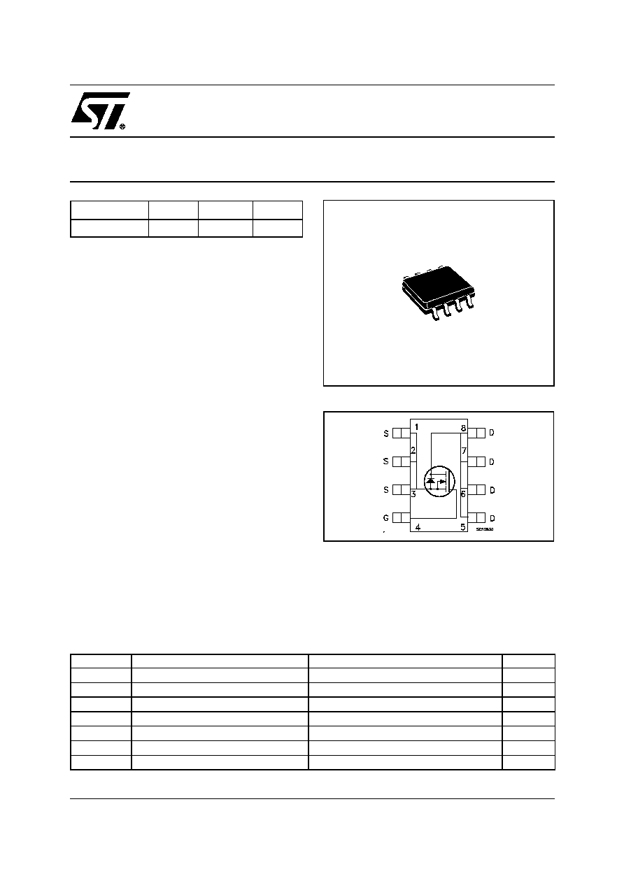
STS17NF3LL
N-CHANNEL 30V - 0.0045
- 17A SO-8
STripFETTM II MOSFET FOR DC-DC CONVERSION
s
TYPICAL R
DS
(on) = 0.0045
@ 10V
s
OPTIMAL R
DS
(on) x Qg TRADE-OFF @ 4.5V
s
CONDUCTION LOSSES REDUCED
s
SWITCHING LOSSES REDUCED
DESCRIPTION
This application specific Power MOSFET is the
second generation of STMicroelectronis unique
"Single Feature SizeTM" strip-based process. The
resulting transistor shows the best trade-off
between on-resistance and gate charge. Such
features make it the best choice in high efficiency
DC-DC converters for Telecom and computer
industries.
APPLICATIONS
s
DC-DC CONVERTERS FOR TELECOM AND
NOTEBOOK CPU CORE
s
SYNCHRONOUS RECTIFIER
TYPE
V
DSS
R
DS(on)
I
D
STS17NF3LL
30 V
<0.0055
17 A
SO-8
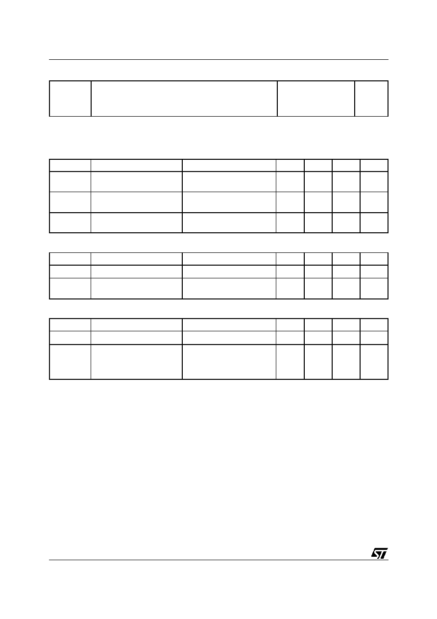
INTERNAL SCHEMATIC DIAGRAM
ABSOLUTE MAXIMUM RATINGS
(
∑)
Pulse width limited by safe operating area.
Symbol
Parameter
Value
Unit
V
DS
Drain-source Voltage (V
GS
= 0)
30
V
V
DGR
Drain-gate Voltage (R
GS
= 20 k
)
30
V
V
GS
Gate- source Voltage
± 18
V
I
D
Drain Current (continuous) at T
C
= 25∞C
17
A
I
D
Drain Current (continuous) at T
C
= 100∞C
12
A
I
DM
(
∑)
Drain Current (pulsed)
68
A
P
tot
Total Dissipation at T
C
= 25∞C
3.2
W
STS17NF3LL
2/8
THERMAL DATA
(*)
When Mounted on 1 inch
2
FR-4 board, 2 oz of Cu and t
[
10 sec.
ELECTRICAL CHARACTERISTICS (T
case
= 25 ∞C unless otherwise specified)
OFF
ON
(*)
DYNAMIC
Rthj-amb
Rthj-lead
T
j
T
stg
(*)
Thermal Resistance Junction-ambient
Thermal Resistance Junction-leads
Maximum Operating Junction Temperature
Storage Temperature
Max
Max
47
16
-55 to 175
-55 to 175
∞C/W
∞C/W
∞C
∞C
Symbol
Parameter
Test Conditions
Min.
Typ.
Max.
Unit
V
(BR)DSS
Drain-source
Breakdown Voltage
I
D
= 250 µA, V
GS
= 0
30
V
I
DSS
Zero Gate Voltage
Drain Current (V
GS
= 0)
V
DS
= Max Rating
V
DS
= Max Rating T
C
= 125∞C
1
10
µA
µA
I
GSS
Gate-body Leakage
Current (V
DS
= 0)
V
GS
= ± 18 V
±100
nA
Symbol
Parameter
Test Conditions
Min.
Typ.
Max.
Unit
V
GS(th)
Gate Threshold Voltage
V
DS
= V
GS
I
D
= 250 µA
1
V
R
DS(on)
Static Drain-source On
Resistance
V
GS
= 10 V
I
D
= 8.5 A
V
GS
= 4.5 V
I
D
= 8.5 A
0.0045
0.0055
0.0055
0.007
Symbol
Parameter
Test Conditions
Min.
Typ.
Max.
Unit
g
fs (*)
Forward Transconductance
V
DS
= 10 V
I
D
= 8.5 A
37
S
C
iss
C
oss
C
rss
Input Capacitance
Output Capacitance
Reverse Transfer
Capacitance
V
DS
= 25V, f = 1 MHz, V
GS
= 0
2160
614
98
pF
pF
pF
3/8
STS17NF3LL
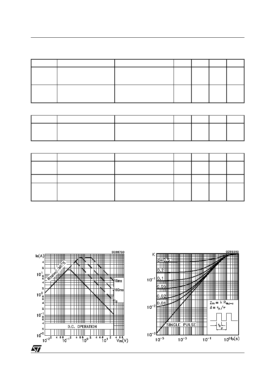
Safe Operating Area
SWITCHING ON
SWITCHING OFF
SOURCE DRAIN DIODE
(*)
Pulsed: Pulse duration = 300 µs, duty cycle 1.5 %.
(
∑)
Pulse width limited by safe operating area.
Symbol
Parameter
Test Conditions
Min.
Typ.
Max.
Unit
t
d(on)
t
r
Turn-on Delay Time
Rise Time
V
DD
= 15 V
I
D
= 8.5 A
R
G
= 4.7
V
GS
= 4.5 V
(Resistive Load, Figure 1)
23.5
39
ns
ns
Q
g
Q
gs
Q
gd
Total Gate Charge
Gate-Source Charge
Gate-Drain Charge
V
DD
=24V I
D
=12.5A V
GS
=4.5 V
(see test circuit, Figure 2)
26
7
12
35
nC
nC
nC
Symbol
Parameter
Test Conditions
Min.
Typ.
Max.
Unit
t
d(off)
t
f
Turn-off Delay Time
Fall Time
V
DD
= 15 V
I
D
= 8.5 A
R
G
= 4.7
,
V
GS
= 4.5 V
(Resistive Load, Figure 3)
47.5
37
ns
ns
Symbol
Parameter
Test Conditions
Min.
Typ.
Max.
Unit
I
SD
I
SDM
(
∑
)
Source-drain Current
Source-drain Current (pulsed)
17
68
A
A
V
SD
(*)
Forward On Voltage
I
SD
= 17 A
V
GS
= 0
1.2
V
t
rr
Q
rr
I
RRM
Reverse Recovery Time
Reverse Recovery Charge
Reverse Recovery Current
I
SD
= 17 A
di/dt = 100A/µs
V
DD
= 15 V
T
j
= 150∞C
(see test circuit, Figure 3)
39
45
2.3
ns
nC
A
ELECTRICAL CHARACTERISTICS (continued)
Thermal Impedance
STS17NF3LL
4/8
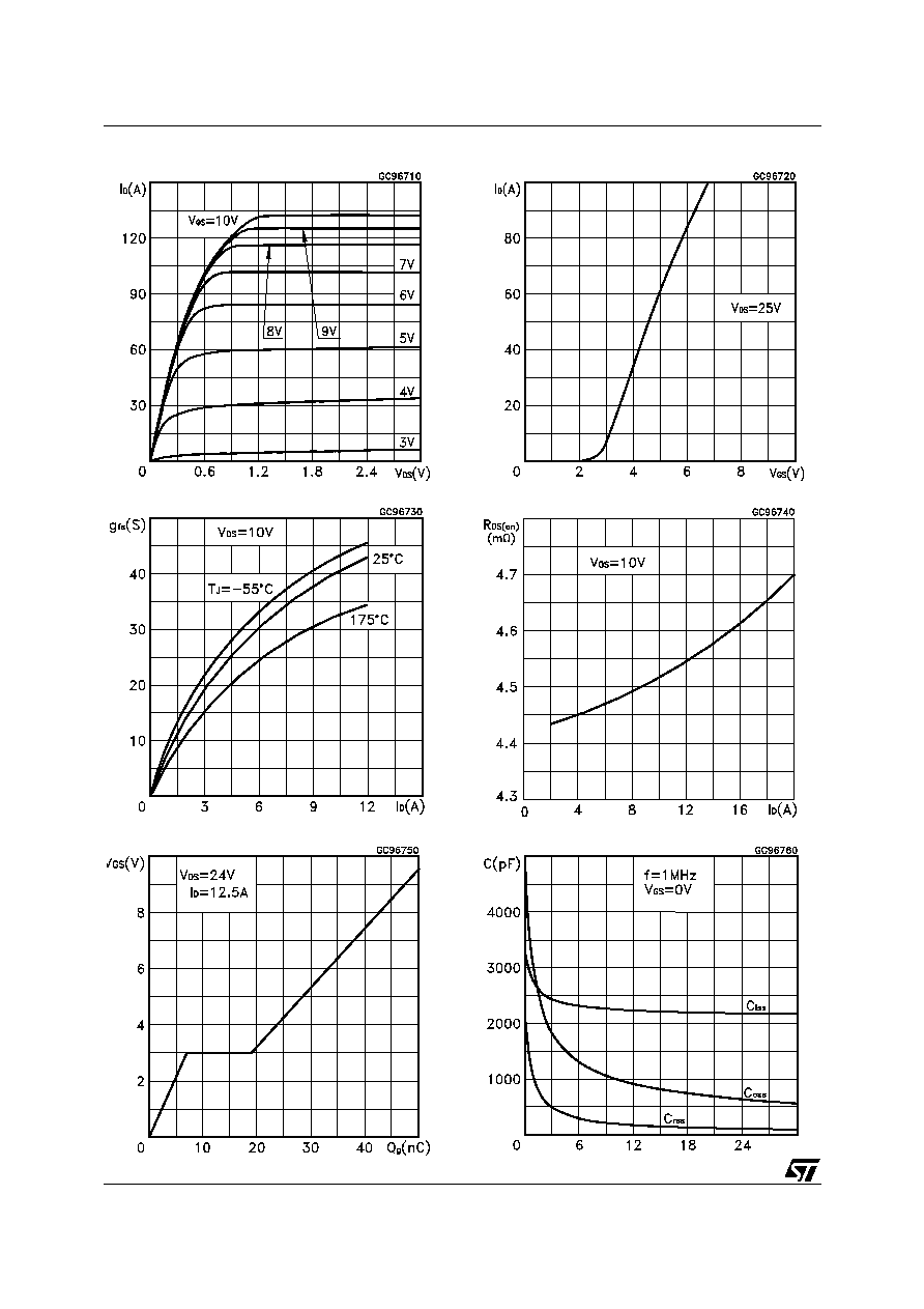
Output Characteristics
Transfer Characteristics
Transconductance
Static Drain-source On Resistance
Gate Charge vs Gate-source Voltage
Capacitance Variations

5/8
STS17NF3LL
.
.
Normalized Gate Threshold Voltage vs Temperature
Normalized on Resistance vs Temperature
Source-drain Diode Forward Characteristics
Normalized Breakdown Voltage vs Temperature.
.
.