
1/9
September 2004
STS3DPF60L
DUAL P-CHANNEL 60V - 0.10
- 3A SO-8
STripFETTM MOSFET
Table 1: General Features
s
TYPICAL R
DS
(on) = 0.10
@ 10V
s
STANDARD OUTLINE FOR EASY
AUTOMATED SURFACE MOUNT
ASSEMBLYY
s
LOW THRESHOLD DRIVE
DESCRIPTION
This MOSFET is the latest development of STMi-
croelectronis unique "Single Feature SizeTM" strip-
based process. The resulting transistor shows ex-
tremely high packing density for low on-resistance,
rugged avalanche characteristics and less critical
alignment steps therefore a remarkable manufac-
turing reproducibility.
APPLICATIONS
s
DC-DC CONVERTERS
Table 2: Order Codes
Figure 1: Package
Figure 2: Internal Schematic Diagram
TYPE
V
DSS
R
DS(on)
I
D
STS3DPF60L
60 V
< 0.12
3 A
SO-8
PART NUMBER
MARKING
PACKAGE
PACKAGING
STS3DPF60L
S3DPF60L
SO-8
TAPE & REEL
Rev. 1

STS3DPF60L
2/9
Table 3: Absolute Maximum ratings
(
∑)
Pulse width limited by safe operating area.
Table 4: Thermal Data
(*)
When Mounted on 1 inch
2
FR-4 board, 2 oz of Cu t
10 s
ELECTRICAL CHARACTERISTICS (T
CASE
=25∞C UNLESS OTHERWISE SPECIFIED)
Table 5: On/Off
Symbol
Parameter
Value
Unit
V
DS
Drain-source Voltage (V
GS
= 0)
60
V
V
DGR
Drain-gate Voltage (R
GS
= 20 k
)
60
V
V
GS
Gate- source Voltage
± 16
V
I
D
Drain Current (continuous) at T
C
= 25∞C
Drain Current (continuous) at T
C
= 100∞C
3
1.9
A
A
I
DM
(
∑)
Drain Current (pulsed)
12
A
P
tot
Total Dissipation at T
C
= 25∞C
2
W
T
stg
Storage Temperature
-55 to 150
∞C
T
j
Operating Junction Temperature
Rthj-amb
(*)Thermal Resistance Junction-ambient
62.5
∞C/W
Symbol
Parameter
Test Conditions
Min.
Typ.
Max.
Unit
V
(BR)DSS
Drain-source
Breakdown Voltage
I
D
= 250 µA, V
GS
= 0
60
V
I
DSS
Zero Gate Voltage
Drain Current (V
GS
= 0)
V
DS
= Max Rating
V
DS
= Max Rating ,T
C
= 125∞C
1
10
µA
µA
I
GSS
Gate-body Leakage
Current (V
DS
= 0)
V
GS
= ± 16 V
±100
nA
V
GS(th)
Gate Threshold Voltage
V
DS
= V
GS
, I
D
= 250 µA
1.5
V
R
DS(on)
Static Drain-source On
Resistance
V
GS
= 10 V, I
D
= 1.5 A
V
GS
= 4.5 V, I
D
= 1.5 A
0.10
0.130
0.12
0.160

3/9
STS3DPF60L
ELECTRICAL CHARACTERISTICS (CONTINUED)
Table 6: Dynamic
Table 7: Source Drain Diode
(*)
Pulsed: Pulse duration = 300 µs, duty cycle 1.5 %.
(∑)
Pulse width limited by safe operating area.
Symbol
Parameter
Test Conditions
Min.
Typ.
Max.
Unit
g
fs
(*)
Forward Transconductance
V
DS
= 10 V, I
D
= 3 A
7.2
S
C
iss
C
oss
C
rss
Input Capacitance
Output Capacitance
Reverse Transfer
Capacitance
V
DS
= 25V f = 1 MHz V
GS
= 0
630
121
49
pF
pF
pF
t
d(on)
t
r
t
d(off)
t
f
Turn-on Delay Time
Rise Time
Turn-off Delay Time
Fall Time
V
DD
= 30 V , I
D
= 1.5 A
R
G
= 4.7
, V
GS
= 4.5 V
(see Figure 16)
124
54
39
14.5
ns
ns
ns
ns
Q
g
Q
gs
Q
gd
Total Gate Charge
Gate-Source Charge
Gate-Drain Charge
V
DD
= 48V, I
D
= 3A V
GS
=4.5V
(see Figure 19)
11.6
4.5
4.7
15.7
nC
nC
nC
Symbol
Parameter
Test Conditions
Min.
Typ.
Max.
Unit
I
SD
I
SDM
(∑)
Source-drain Current
Source-drain Current (pulsed)
3
12
A
A
V
SD
(*)
Forward On Voltage
I
SD
= 3 A, V
GS
= 0
1.2
V
t
rr
Q
rr
I
RRM
Reverse Recovery Time
Reverse Recovery Charge
Reverse Recovery Current
I
SD
= 3 A, di/dt = 100A/µs
V
DD
= 30 V, T
j
= 150∞C
(see Figure 17)
44
68.2
3.1
ns
nC
A
STS3DPF60L
4/9
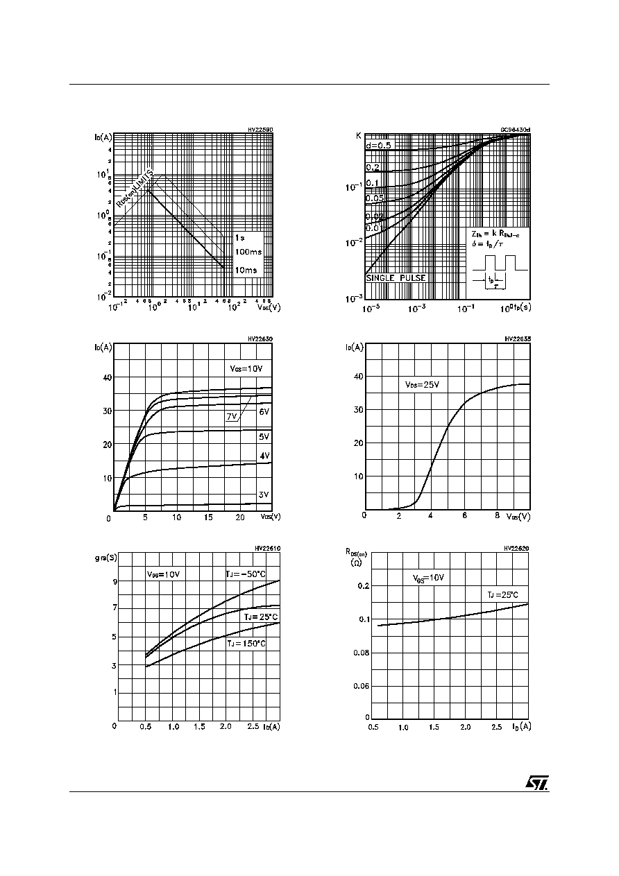
Figure 3: Safe Operating Area
Figure 4: Output Characteristics
Figure 5: Transconductance
Figure 6: Thermal Impedance
Figure 7: Transfer Characteristics
Figure 8: Static Drain-source On Resistance

5/9
STS3DPF60L
Figure 9: Gate Charge vs Gate-source Voltage
Figure 10: Normalized Gate Thereshold Volt-
age vs Temperature
Figure 11: Dource-Drain Diode Forward Char-
acteristics
Figure 12: Capacitance Variations
Figure 13: Normalized On Resistance vs Tem-
perature
Figure 14: Normalized Breakdown Voltage vs
Temperature