 | –≠–ª–µ–∫—Ç—Ä–æ–Ω–Ω—ã–π –∫–æ–º–ø–æ–Ω–µ–Ω—Ç: STS6PF30L | –°–∫–∞—á–∞—Ç—å:  PDF PDF  ZIP ZIP |
1/8
May 2003
.
STS6PF30L
P-CHANNEL 30V - 0.027
- 6A SO-8
STripFETTM POWER MOSFET
s
TYPICAL R
DS
(on) = 0.027
s
STANDARD OUTLINE FOR EASY
AUTOMATED SURFACE MOUNT ASSEMBLY
s
LOW THRESHOLD DRIVE
DESCRIPTION
This Power MOSFET is the latest development of
STMicroelectronis unique "Single Feature SizeTM"
strip-based process. The resulting transistor
shows extremely high packing density for low on-
resistance, rugged avalanche characteristics and
less critical alignment steps therefore a remark-
able manufacturing reproducibility.
APPLICATIONS
s
MOBILE PHONE APPLICATIONS
s
DC-DC CONVERTERS
s
BATTERY MANAGEMENT IN NOMADIC
EQUIPMENT
TYPE
V
DSS
R
DS(on)
I
D
STS6PF30L
30 V
<0.030
6 A
Information furnished is believed to be accurate and reliable. However, STMicroel
of use of such information nor for any infringement of patents or other rights of third
by implication or otherwise under any patent or patent rights of STMicroelectronic
to change without notice. This publication supersedes and replaces all information
authorized for use as critical components in life support devices or systems withou
The ST logo is registered trademark of ST
Æ
2003 STMicroelectronics - All Righ
All other names are the property of their re
STMicroelectronics GROUP OF CO
Australia - Brazil - China - Finland - France - Germany - Hong Kong - In
Singapore - Spain - Sweden - Switzerland - Un
http://www.st.com
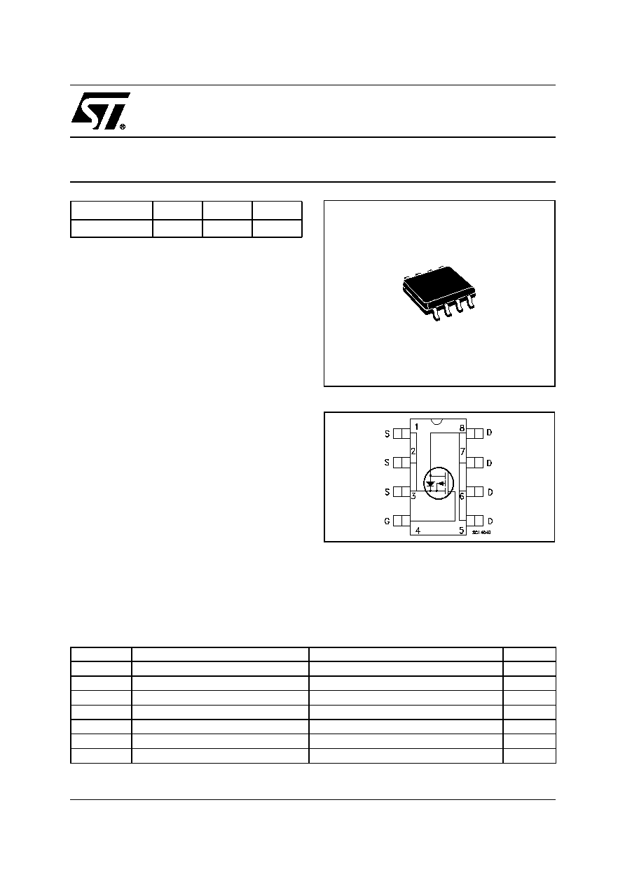
SO-8
ABSOLUTE MAXIMUM RATINGS
(
∑)
Pulse width limited by safe operating area.
Note: For the P-CHANNEL MOSFET actual polarity of
voltages and current has to be reversed
Symbol
Parameter
Value
Unit
V
DS
Drain-source Voltage (V
GS
= 0)
30
V
V
DGR
Drain-gate Voltage (R
GS
= 20 k
)
30
V
V
GS
Gate- source Voltage
± 16
V
I
D
Drain Current (continuous) at T
C
= 25∞C
6
A
I
D
Drain Current (continuous) at T
C
= 100∞C
3.8
A
I
DM
(
∑)
Drain Current (pulsed)
24
A
P
tot
Total Dissipation at T
C
= 25∞C
2.5
W
INTERNAL SCHEMATIC DIAGRAM

STS6PF30L
2/8
THERMAL DATA
ELECTRICAL CHARACTERISTICS (T
case
= 25 ∞C unless otherwise specified)
OFF
ON
(*)
DYNAMIC
Rthj-amb
T
j
T
stg
Thermal Resistance Junction-ambient
Maximum Lead Temperature For Soldering Purpose
storage temperature
Max
Typ
50
150
-55 to 150
∞C/W
∞C
∞C
Symbol
Parameter
Test Conditions
Min.
Typ.
Max.
Unit
V
(BR)DSS
Drain-source
Breakdown Voltage
I
D
= 250 µA, V
GS
= 0
30
V
I
DSS
Zero Gate Voltage
Drain Current (V
GS
= 0)
V
DS
= Max Rating
V
DS
= Max Rating T
C
= 125∞C
1
10
µA
µA
I
GSS
Gate-body Leakage
Current (V
DS
= 0)
V
GS
= ± 16 V
±100
nA
Symbol
Parameter
Test Conditions
Min.
Typ.
Max.
Unit
V
GS(th)
Gate Threshold Voltage
V
DS
= V
GS
I
D
= 250 µA
1
1.6
2.5
V
R
DS(on)
Static Drain-source On
Resistance
V
GS
= 10 V
I
D
= 3 A
V
GS
= 5 V
I
D
= 3 A
0.027
0.034
0.030
0.042
Symbol
Parameter
Test Conditions
Min.
Typ.
Max.
Unit
g
fs (*)
Forward Transconductance
V
DS
=10 V
I
D
=3 A
12
S
C
iss
C
oss
C
rss
Input Capacitance
Output Capacitance
Reverse Transfer
Capacitance
V
DS
= 25V, f = 1 MHz, V
GS
= 0
1670
345
120
pF
pF
pF

3/8
STS6PF30L
SWITCHING ON
(*)
SWITCHING OFF
(*)
SOURCE DRAIN DIODE
(*)
(*)
Pulse width
[
300 µs, duty cycle 1.5 %.
(
∑)
Pulse width limited by T
JMAX
Symbol
Parameter
Test Conditions
Min.
Typ.
Max.
Unit
t
d(on)
t
r
Turn-on Delay Time
Rise Time
V
DD
= 15 V
I
D
= 3 A
R
G
= 4.7
V
GS
= 5 V
(Resistive Load, Figure 1)
62
140
ns
ns
Q
g
Q
gs
Q
gd
Total Gate Charge
Gate-Source Charge
Gate-Drain Charge
V
DD
= 24V I
D
= 6A V
GS
=5V
(see test circuit, Figure 2)
21
3.9
8.6
28
nC
nC
nC
Symbol
Parameter
Test Conditions
Min.
Typ.
Max.
Unit
t
d(off)
t
f
Turn-off Delay Time
Fall Time
V
DD
= 24 V
I
D
= 3 A
R
G
= 4.7
,
V
GS
= 5 V
(Resistive Load, Figure 1)
57
19
ns
ns
Symbol
Parameter
Test Conditions
Min.
Typ.
Max.
Unit
I
SD
I
SDM
(
∑
)
Source-drain Current
Source-drain Current (pulsed)
6
4
A
A
V
SD
(*)
Forward On Voltage
I
SD
= 6 A
V
GS
= 0
1.2
V
t
rr
Q
rr
I
RRM
Reverse Recovery Time
Reverse Recovery Charge
Reverse Recovery Current
I
SD
= 6 A
di/dt = 100A/µs
V
DD
= 15 V
T
j
= 150∞C
(see test circuit, Figure 3)
37
46.3
2.5
ns
nC
A
ELECTRICAL CHARACTERISTICS (continued)
Safe Operating Area
Thermal Impedance
STS6PF30L
4/8
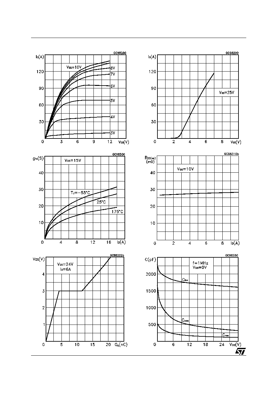
Output Characteristics
Transfer Characteristics
Transconductance
Static Drain-source On Resistance
Gate Charge vs Gate-source Voltage
Capacitance Variations

5/8
STS6PF30L
Normalized Gate Threshold Voltage vs Temperature
Normalized on Resistance vs Temperature
Source-drain Diode Forward Characteristics
Normalized Breakdown Voltage vs Temperature
.
.