 | ÐлекÑÑоннÑй компоненÑ: STS7NF30L | СкаÑаÑÑ:  PDF PDF  ZIP ZIP |
Äîêóìåíòàöèÿ è îïèñàíèÿ www.docs.chipfind.ru
STS7NF30L
N - CHANNEL 30V - 0.021
- 7A SO-8
STripFET
TM
POWER MOSFET
PRELIMINARY DATA
s
TYPICAL R
DS(on)
= 0.021
s
STANDARD OUTLINE FOR EASY
AUTOMATED SURFACE MOUNT ASSEMBLY
s
LOW THRESHOLD DRIVE
DESCRIPTION
This Power MOSFET is the second generation of
STMicroelectronics unique " Single Feature
Size
TM
"
strip-based process. The resulting
transistor shows extremely high packing density
for low on-resistance, rugged avalanche
characteristics and less critical alignment steps
therefore a remarkable manufacturing
reproducibility.
APPLICATIONS
s
DC MOTOR DRIVE
s
DC-DC CONVERTERS
s
BATTERY MANAGMENT IN NOMADIC
EQUIPMENT
s
POWER MANAGEMENT IN
PORTABLE/DESKTOP PC
s
®
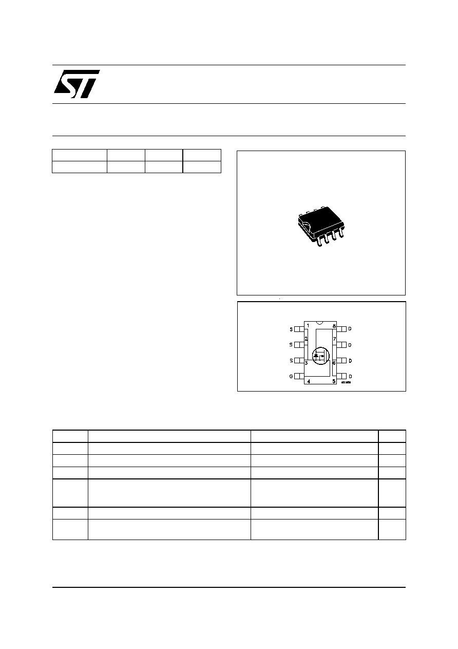
INTERNAL SCHEMATIC DIAGRAM
May 1999
SO-8
ABSOLUTE MAXIMUM RATINGS
Symbol
Parameter
Value
Unit
V
DS
Drain-source Voltage (V
GS
= 0)
30
V
V
DGR
Drain- gate Voltage (R
GS
= 20 k
)
30
V
V
GS
Gate-source Voltage
±
20
V
I
D
Drain Current (continuous) at Tc = 25
o
C
Drain Current (continuous) at T
c
= 100
o
C
7
4.4
A
A
I
DM
(
·
)
Drain Current (pulsed)
42
A
P
tot
Total Dissipation at T
c
= 25
o
C
2.5
W
(
·
) Pulse width limited by safe operating area
TYPE
V
DSS
R
DS(on)
I
D
STS7NF30L
30 V
< 0.025
7 A
1/5
THERMAL DATA
R
thj-amb
Tj
Tstg
(*)Thermal Resistance Junction-ambient
Maximum Operating Junction Temperature
Storage Temperature
50
150
-55 to 150
o
C/W
o
C
o
C
(*) Mounted on FR-4 board ( (t
10
sec)
ELECTRICAL CHARACTERISTICS (T
case
= 25
o
C unless otherwise specified)
OFF
Symbol
Parameter
Test Conditions
Min.
Typ.
Max.
Unit
V
(BR)DSS
Drain-source
Breakdown Voltage
I
D
= 250
µ
A V
GS
= 0
30
V
I
DSS
Zero Gate Voltage
Drain Current (V
GS
= 0)
V
DS
= Max Rating
V
DS
= Max Rating T
c
= 125
o
C
1
10
µ
A
µ
A
I
GSS
Gate-body Leakage
Current (V
DS
= 0)
V
GS
=
±
20 V
±
100
nA
ON (
)
Symbol
Parameter
Test Conditions
Min.
Typ.
Max.
Unit
V
GS(th)
Gate Threshold Voltage V
DS
= V
GS
I
D
= 250
µ
A
1
1.6
2.5
V
R
DS(on)
Static Drain-source On
Resistance
V
GS
= 10 V I
D
= 3.5 A
V
GS
= 4.5 V I
D
= 3.5 A
0.021
0.025
0.025
0.032
I
D(o n)
On State Drain Current
V
DS
> I
D(o n)
x R
DS(on )max
V
GS
= 10 V
20
A
DYNAMIC
Symbol
Parameter
Test Conditions
Min.
Typ.
Max.
Unit
g
fs
(
)
Forward
Transconductance
V
DS
> I
D(o n)
x R
DS(on )max
I
D
= 3.5 A
10
S
C
iss
C
oss
C
rss
Input Capacitance
Output Capacitance
Reverse Transfer
Capacitance
V
DS
= 25 V f = 1 MHz V
GS
= 0 V
1250
230
50
pF
pF
pF
STS7NF30L
2/5
ELECTRICAL CHARACTERISTICS (continued)
SWITCHING ON
Symbol
Parameter
Test Conditions
Min.
Typ.
Max.
Unit
t
d(on )
t
r
Turn-on Delay Time
Rise Time
V
DD
= 15 V I
D
= 3 A
R
G
= 4.7
V
GS
= 5 V
(Resistive Load, see fig. 3)
22
30
ns
ns
Q
g
Q
gs
Q
gd
Total Gate Charge
Gate-Source Charge
Gate-Drain Charge
V
DD
= 24 V I
D
= 7 A V
GS
= 4.5 V
17
4
6
23
nC
nC
nC
SWITCHING OFF
Symbol
Parameter
Test Conditions
Min.
Typ.
Max.
Unit
t
d(of f)
t
f
Turn-off Delay Time
Fall Time
V
DD
= 15 V I
D
= 3 A
R
G
= 4.7
V
GS
= 5 V
(Resistive Load, see fig. 3)
55
10
ns
ns
t
r(Voff)
t
f
t
c
Off-voltage Rise Time
Fall Time
Cross-over Time
V
clamp
= 24 V I
D
= 7 A
R
G
= 4.7
V
GS
= 5 V
(Inductive Load, see fig. 5)
10
18
30
ns
ns
ns
SOURCE DRAIN DIODE
Symbol
Parameter
Test Conditions
Min.
Typ.
Max.
Unit
I
SD
I
SDM
(
·
)
Source-drain Current
Source-drain Current
(pulsed)
2
8
A
A
V
SD
(
)
Forward On Voltage
I
SD
= 7 A V
GS
= 0
1.2
V
t
rr
Q
rr
I
RRM
Reverse Recovery
Time
Reverse Recovery
Charge
Reverse Recovery
Current
I
SD
= 7 A di/dt = 100 A/
µ
s
V
DD
= 20 V T
j
= 150
o
C
(see test circuit, fig. 5)
30
30
2
ns
nC
A
(
) Pulsed: Pulse duration = 300
µ
s, duty cycle 1.5 %
(
·
) Pulse width limited by safe operating area
STS7NF30L
3/5
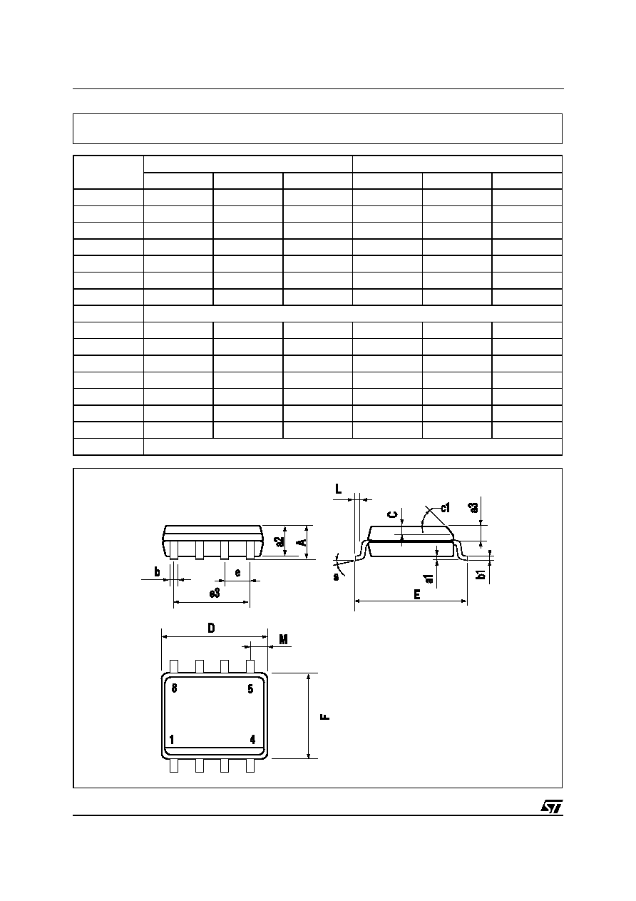
DIM.
mm
inch
MIN.
TYP.
MAX.
MIN.
TYP.
MAX.
A
1.75
0.068
a1
0.1
0.25
0.003
0.009
a2
1.65
0.064
a3
0.65
0.85
0.025
0.033
b
0.35
0.48
0.013
0.018
b1
0.19
0.25
0.007
0.010
C
0.25
0.5
0.010
0.019
c1
45 (typ.)
D
4.8
5.0
0.188
0.196
E
5.8
6.2
0.228
0.244
e
1.27
0.050
e3
3.81
0.150
F
3.8
4.0
0.14
0.157
L
0.4
1.27
0.015
0.050
M
0.6
0.023
S
8 (max.)
0016023
SO-8 MECHANICAL DATA
STS7NF30L
4/5
Information furnished is believed to be accurate and reliable. However, STMicroelectronics assumes no responsibility for the consequences
of use of such information nor for any infringement of patents or other rights of third parties which may result from its use. No license is
granted by implication or otherwise under any patent or patent rights of STMicroelectronics. Specification mentioned in this publication are
subject to change without notice. This publication supersedes and replaces all information previously supplied. STMicroelectronics products
are not authorized for use as critical components in life support devices or systems without express written approval of STMicroelectronics.
The ST logo is a trademark of STMicroelectronics
© 1999 STMicroelectronics Printed in Italy All Rights Reserved
STMicroelectronics GROUP OF COMPANIES
Australia - Brazil - Canada - China - France - Germany - Italy - Japan - Korea - Malaysia - Malta - Mexico - Morocco - The Netherlands -
Singapore - Spain - Sweden - Switzerland - Taiwan - Thailand - United Kingdom - U.S.A.
http://www.st.com
.
STS7NF30L
5/5