
1/9
June 2004
STS8DNH3LL
DUAL N-CHANNEL 30V - 0.018
- 8A SO-8
LOW GATE CHARGE STripFETTM III POWER MOSFET
Rev.0.2
TYPICAL R
DS
(on) = 0.018
OPTIMAL R
DS
(on) x Qg TRADE-OFF @ 4.5V
CONDUCTION LOSSES REDUCED
SWITCHING LOSSES REDUCED
DESCRIPTION
This application specific MOSFET is the Third generation
of STMicroelectronis unique "Single Feature SizeTM"
strip-based process. The resulting transistor shows the
best trade-off between on-resistance and gate charge.
When used as high and low side in buck regulators, it
gives the best performance in terms of both conduction
and switching losses. This is extremely important for
motherboards where fast switching and high efficiency
are of paramount importance.
APPLICATIONS
SPECIFICALLY DESIGNED AND OPTIMISED
FOR HIGH EFFICIENCY CPU CORE DC/DC
CONVERTERS FOR MOBILE PC
S
Ordering Information
TYPE
V
DSS
R
DS(on)
I
D
STS8DNH3LL
30 V
<0.022
8 A
SALES TYPE
MARKING
PACKAGE
PACKAGING
STS8DNH3LL
S8DNH3LL
SO-8
TAPE & REEL
SO-8
ABSOLUTE MAXIMUM RATINGS
(
∑)
Pulse width limited by safe operating area.
Symbol
Parameter
Value
Unit
V
DS
Drain-source Voltage (V
GS
= 0)
30
V
V
DGR
Drain-gate Voltage (R
GS
= 20 k
)
30
V
V
GS
Gate- source Voltage
± 16
V
I
D
Drain Current (continuous) at T
C
= 25∞C
8
A
I
D
Drain Current (continuous) at T
C
= 100∞C
5
A
I
DM
(
∑)
Drain Current (pulsed)
32
A
P
tot
Total Dissipation at T
C
= 25∞C
2
W
INTERNAL SCHEMATIC DIAGRAM
STS8DNH3LL
2/9
TAB.1 THERMAL DATA
(*)
When mounted on 1 inch
2
FR-4 board, 2 oz of Cu, t
10s
ELECTRICAL CHARACTERISTICS (T
j
= 25 ∞C unless otherwise specified)
TAB.2 OFF
TAB.3 ON
(*)
TAB.4 DYNAMIC
Rthj-amb
T
j
T
stg
(*)
Thermal Resistance Junction-ambient
Maximum Operating Junction Temperature
Storage Temperature
Max
62.5
150
-55 to 150
∞C/W
∞C
∞C
Symbol
Parameter
Test Conditions
Min.
Typ.
Max.
Unit
V
(BR)DSS
Drain-source
Breakdown Voltage
I
D
= 250 µA, V
GS
= 0
30
V
I
DSS
Zero Gate Voltage
Drain Current (V
GS
= 0)
V
DS
= Max Rating
V
DS
= Max Rating T
C
= 125∞C
1
10
µA
µA
I
GSS
Gate-body Leakage
Current (V
DS
= 0)
V
GS
= ± 16 V
±100
nA
Symbol
Parameter
Test Conditions
Min.
Typ.
Max.
Unit
V
GS(th)
Gate Threshold Voltage
V
DS
= V
GS
I
D
= 250 µA
1
V
R
DS(on)
Static Drain-source On
Resistance
V
GS
= 10 V
I
D
= 4 A
V
GS
= 4.5 V
I
D
= 4 A
0.018
0.020
0.022
0.025
Symbol
Parameter
Test Conditions
Min.
Typ.
Max.
Unit
g
fs (*)
Forward Transconductance
V
DS
=15 V
I
D
= 4 A
8.5
S
C
iss
C
oss
C
rss
Input Capacitance
Output Capacitance
Reverse Transfer
Capacitance
V
DS
= 25V, f = 1 MHz, V
GS
= 0
857
147
20
pF
pF
pF

3/9
STS8DNH3LL
TAB.5 SWITCHING ON
TAB.6 SWITCHING OFF
TAB.7 SOURCE DRAIN DIODE
(*)
Pulsed: Pulse duration = 300 µs, duty cycle 1.5 %.
(
∑)
Pulse width limited by safe operating area.
Symbol
Parameter
Test Conditions
Min.
Typ.
Max.
Unit
t
d(on)
t
r
Turn-on Delay Time
Rise Time
V
DD
= 15 V
I
D
= 4 A
R
G
= 4.7
V
GS
= 10 V
(Resistive Load, Figure 1)
12
14.5
ns
ns
Q
g
Q
gs
Q
gd
Total Gate Charge
Gate-Source Charge
Gate-Drain Charge
V
DD
= 15 V I
D
= 8 A V
GS
= 4.5 V
(see test circuit, Figure 2)
7.0
2.5
2.3
10
nC
nC
nC
Symbol
Parameter
Test Conditions
Min.
Typ.
Max.
Unit
t
d(off)
t
f
Turn-off Delay Time
Fall Time
V
DD
= 15 V
I
D
= 4 A
R
G
= 4.7
,
V
GS
= 10 V
(Resistive Load, Figure 1)
23
8
ns
ns
Symbol
Parameter
Test Conditions
Min.
Typ.
Max.
Unit
I
SD
I
SDM
(
∑
)
Source-drain Current
Source-drain Current (pulsed)
8
32
A
A
V
SD
(*)
Forward On Voltage
I
SD
= 4 A V
GS
= 0
1.5
V
t
rr
Q
rr
I
RRM
Reverse Recovery Time
Reverse Recovery Charge
Reverse Recovery Current
I
SD
= 8 A
di/dt = 100A/µs
V
DD
= 15 V
T
j
= 150∞C
(see test circuit, Figure 3)
15
5.7
0.76
ns
nC
A
ELECTRICAL CHARACTERISTICS (continued)
Safe Operating Area
Thermal Impedance

STS8DNH3LL
4/9
Output Characteristics
Transfer Characteristics
Transconductance
Static Drain-source On Resistance
Gate Charge vs Gate-source Voltage
Capacitance Variations
5/9
STS8DNH3LL
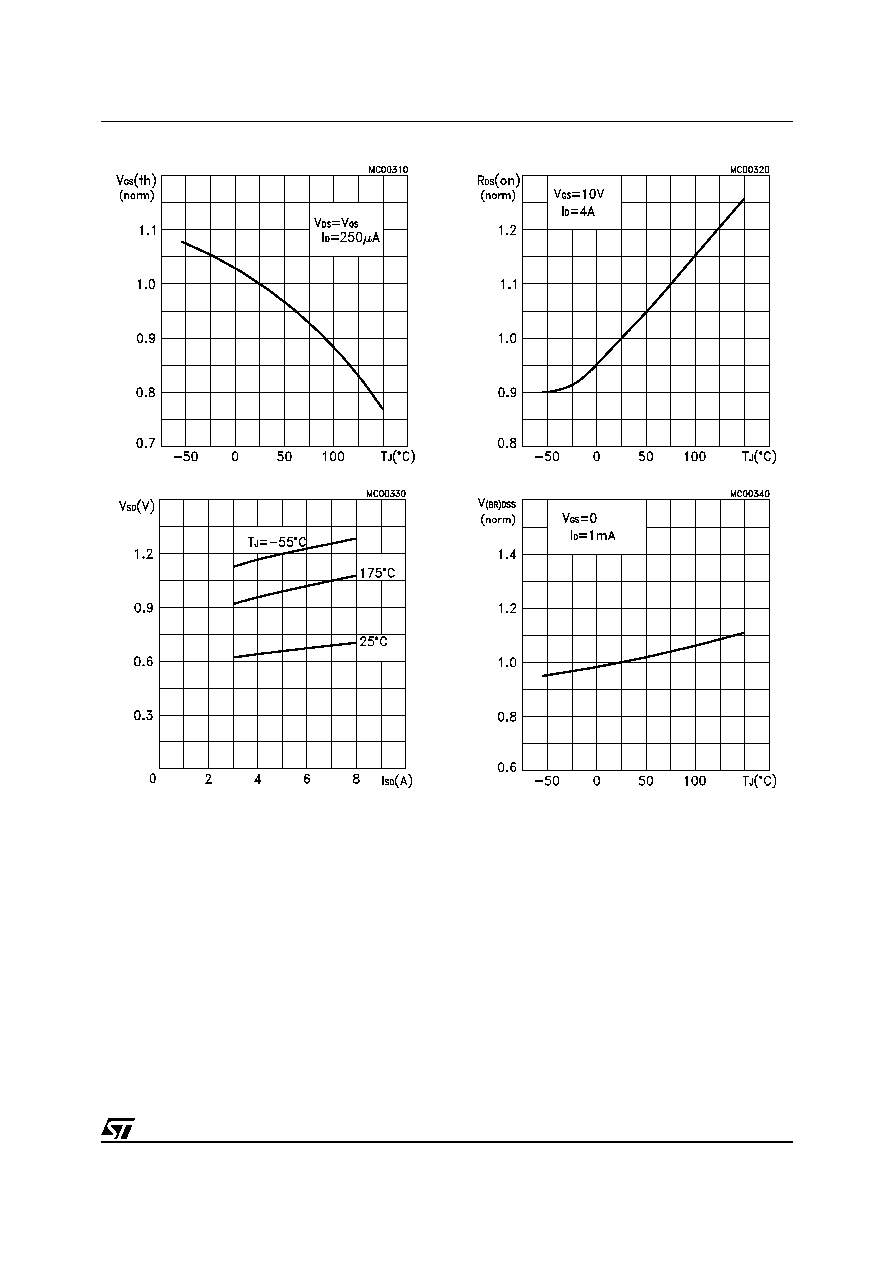
Normalized Gate Threshold Voltage vs Temperature
Normalized
on Resistance vs Temperature
Source-drain Diode Forward Characteristics
Normalized Breakdown Voltage Temperature
.
.
.