 | –≠–ª–µ–∫—Ç—Ä–æ–Ω–Ω—ã–π –∫–æ–º–ø–æ–Ω–µ–Ω—Ç: STU16NB50 | –°–∫–∞—á–∞—Ç—å:  PDF PDF  ZIP ZIP |

STU16NB50
N-CHANNEL 500V - 0.28
- 15.6A-Max220
PowerMESH
TM
MOSFET
s
TYPICAL R
DS(on)
= 0.28
s
EXTREMELY HIGH dv/dt CAPABILITY
s
100% AVALANCHE TESTED
s
VERY LOW INTRINSIC CAPACITANCES
s
GATE CHARGE MINIMIZED
s
±
30V GATE TO SOURCE VOLTAGE RATING
DESCRIPTION
Using the latest high voltage MESH OVERLAY
TM
process, STMicroelectronics has designed an
advanced family
of
power MOSFETs
with
outstanding performances.
The
new
patent
pending strip layout coupled with the Company's
proprietary edge termination structure, gives the
lowest R
DS(on)
per area, exceptional avalanche
and dv/dt capabilities and unrivalled gate charge
and switching characteristics.
APPLICATIONS
s
SWITCH MODE POWER SUPPLIES (SMPS)
s
DC-AC CONVERTERS FOR WELDING
EQUIPMENT AND UNINTERRUPTIBLE
POWER SUPPLIES AND MOTOR DRIVE
This is preliminary information on a new product now in development or undergoing evaluation. Details are subject to change without notice.
Æ
INTERNAL SCHEMATIC DIAGRAM
ABSOLUTE MAXIMUM RATINGS
Symbol
Parameter
Value
Un it
V
DS
Drain-source Voltage (V
GS
= 0)
500
V
V
DGR
Drain- gate Volt age (R
GS
= 20 k
)
500
V
V
GS
G ate-source Voltage
±
30
V
I
D
Drain Current (continuous) at T
c
= 25
o
C
15.6
A
I
D
Drain Current (continuous) at T
c
= 100
o
C
9.8
A
I
DM
(
∑
)
Drain Current (pulsed)
62
A
P
tot
T otal Dissipation at T
c
= 25
o
C
160
W
Derating Factor
1.28
W /
o
C
dv/dt (
1
)
Peak Diode Recovery volt age slope
4.5
V/ns
T
s tg
Storage Temperat ure
-65 to 150
o
C
T
j
Max. Operating Junction Temperature
150
o
C
(
∑
) Pulse width limited by safe operating area
(
1
) I
SD
16A, di/dt
200 A/
µ
s, V
DD
V
( BR)DSS
, Tj
T
JMAX
September 1999
TYPE
V
DSS
R
DS(on)
I
D
ST U16NB50
500 V
< 0. 33
15.6 A
1
2
3
Max220
1/6
THERMAL DATA
R
thj -case
Rthj -amb
R
thc-sink
T
l
Thermal Resistance Junction-case
Max
Thermal Resistance Junction-ambient
Max
Thermal Resistance Case-sink
Typ
Maximum Lead Temperature For Soldering Purpose
0.78
62. 5
0. 5
300
o
C/W
oC/ W
o
C/W
o
C
AVALANCHE CHARACTERISTICS
Symbo l
Parameter
Max Valu e
Unit
I
AR
Avalanche Current , Repet itive or Not-Repet itive
(pulse width limited by T
j
max)
15. 6
A
E
AS
Single Pulse Avalanche Energy
(starting T
j
= 25
o
C, I
D
= I
AR
, V
DD
= 50 V)
850
mJ
ELECTRICAL CHARACTERISTICS (T
case
= 25
o
C unless otherwise specified)
OFF
Symbo l
Parameter
Test Con ditions
Min.
T yp.
Max.
Unit
V
(BR)DSS
Drain-source
Breakdown Voltage
I
D
= 250
µ
A
V
GS
= 0 @ 100
o
C
500
V
I
DSS
Zero G ate Voltage
Drain Current (V
GS
= 0)
V
DS
= Max Rating
V
DS
= Max Rating
T
c
= 125
o
C
1
50
µ
A
µ
A
I
G SS
Gat e-body Leakage
Current (V
DS
= 0)
V
GS
=
±
30 V
±
100
nA
ON (
)
Symbo l
Parameter
Test Con ditions
Min.
T yp.
Max.
Unit
V
G S(th)
Gat e Threshold
Voltage
V
DS
= V
GS
I
D
= 250
µ
A
3
4
5
V
R
DS(on)
Static Drain-source O n
Resist ance
V
GS
= 10V
I
D
=7.8 A
0.28
0.33
I
D(o n)
On Stat e Drain Current
V
DS
> I
D(o n)
x R
DS(on )ma x
V
GS
= 10 V
15. 6
A
DYNAMIC
Symbo l
Parameter
Test Con ditions
Min.
T yp.
Max.
Unit
g
f s
(
)
Forward
Transconduct ance
V
DS
> I
D(o n)
x R
DS(on )ma x
I
D
=7.8 A
9
S
C
iss
C
os s
C
rss
Input Capacitance
Out put Capacitance
Reverse T ransfer
Capacitance
V
DS
= 25 V
f = 1 MHz
V
GS
= 0
2850
400
42
3710
520
55
pF
pF
pF
STU16NB50
2/6

ELECTRICAL CHARACTERISTICS (continued)
SWITCHING ON
Symbo l
Parameter
Test Con ditions
Min.
T yp.
Max.
Unit
t
d(on)
t
r
Turn-on Time
Rise Time
V
DD
= 250 V
I
D
= 7.8 A
R
G
= 4.7
V
G S
= 10 V
30
15
42
21
ns
ns
Q
g
Q
gs
Q
gd
Tot al Gate Charge
Gat e-Source Charge
Gat e-Drain Charge
V
DD
= 400 V
I
D
=15.6 A V
GS
= 10 V
67
20
30
88
nC
nC
nC
SWITCHING OFF
Symbo l
Parameter
Test Con ditions
Min.
T yp.
Max.
Unit
t
r (Voff)
t
f
t
c
Off -volt age Rise Time
Fall Time
Cross-over Time
V
DD
= 400 V
I
D
= 15. 6 A
R
G
= 4.7
V
GS
= 10 V
20
15
35
26
21
49
ns
ns
ns
SOURCE DRAIN DIODE
Symbo l
Parameter
Test Con ditions
Min.
T yp.
Max.
Unit
I
SD
I
SDM
(
∑
)
Source-drain Current
Source-drain Current
(pulsed)
15. 6
62
A
A
V
SD
(
)
Forward On Volt age
I
SD
= 15.6 A
V
GS
= 0
1. 6
V
t
rr
Q
rr
I
RRM
Reverse Recovery
Time
Reverse Recovery
Charge
Reverse Recovery
Current
I
SD
= 15. 6 A
di/dt = 100 A/
µ
s
V
DD
= 100 V
T
j
= 150
o
C
600
6.8
22.5
ns
µ
C
A
(
) Pulsed: Pulse duration = 300
µ
s, duty cycle 1.5 %
(
∑
) Pulse width limited by safe operating area
STU16NB50
3/6

Fig. 1: Unclamped Inductive Load Test Circuit
Fig. 2: Unclamped Inductive Waveform
Fig. 5: Test Circuit For Inductive Load Switching
And Diode Recovery Times
Fig. 3: Switching Times Test Circuits For
Resistive Load
Fig. 4: Gate Charge test Circuit
STU16NB50
4/6
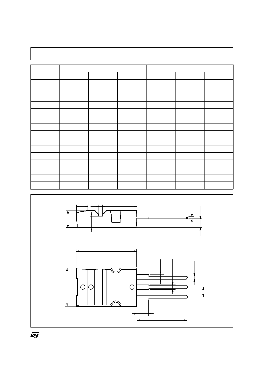
DIM.
mm
inch
MIN.
TYP.
MAX.
MIN.
TYP.
MAX.
A
4.3
4.6
0.169
0.181
A1
2.2
2.4
0.087
0.094
A2
2.9
3.1
0.114
0.122
b
0.7
0.93
0.027
0.036
b1
1.25
1.4
0.049
0.055
b2
1.2
1.38
0.047
0.054
c
0.45
0.6
0.18
0.023
D
15.9
16.3
0.626
0.641
D1
9
9.35
0.354
0.368
D2
0.8
1.2
0.031
0.047
D3
2.8
3.2
0.110
0.126
e
2.44
2.64
0.096
0.104
E
10.05
10.35
0.396
0.407
L
13.2
13.6
0.520
0.535
L1
3
3.4
0.118
0.133
A
A2
A1
C
D3
D1
D2
D
b1
b2
b
E
L
L1
e
P011R
Max220 MECHANICAL DATA
STU16NB50
5/6