1/11
July 2005
STP4N150
STW4N150
N-CHANNEL 1500V - 5
- 4A TO-220/TO-247
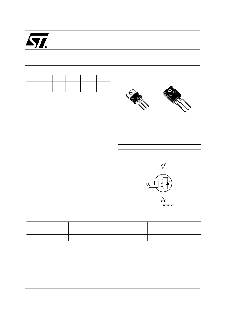
Very High Voltage PowerMESHTM MOSFET
Table 1: General Features
s
TYPICAL R
DS
(on) = 5
s
AVALANCHE RUGGEDNESS
s
GATE CHARGE MINIMIZED
s
VERY LOW INTRINSIC CAPACITANCES
s
HIGH SPEED SWITCHING
DESCRIPTION
Using the well consolidated high voltage MESH
OVERLAYTM process, STMicroelectronics has de-
signed an advanced family of Power MOSFETs
with outstanding performances. The strengthened
layout coupled with the Company's proprietary
edge termination structure, gives the lowest
RDS(on) per area, unrivalled gate charge and
switching characteristics.
APPLICATIONS
s
SWITCH MODE POWER SUPPLIES
Table 2: Order Codes
Figure 1: Package
Figure 2: Internal Schematic Diagram
TYPE
V
DSS
R
DS(on)
I
D
Pw
STP4N150
STW4N150
1500 V
1500 V
< 7
< 7
4 A
4 A
160 W
160 W
TO-220
1
2
3
TO-247
1
2
3
SALES TYPE
MARKING
PACKAGE
PACKAGING
STP4N150
P4N150
TO-220
TUBE
STW4N150
W4N150
TO-247
TUBE
Rev. 3
STP4N150 - STW4N150
2/11
Table 3: Absolute Maximum ratings
( ) Pulse width limited by safe operating area
(*) Limited only by maximum temperature allowed
Table 4: Thermal Data
Table 5: Avalanche Characteristics
ELECTRICAL CHARACTERISTICS (T
CASE
=25∞C UNLESS OTHERWISE SPECIFIED)
Table 6: On /Off
Symbol
Parameter
Value
Unit
V
DS
Drain-source Voltage (V
GS
= 0)
1500
V
V
DGR
Drain-gate Voltage (R
GS
= 20 k
)
1500
V
V
GS
Gate- source Voltage
± 30
V
I
D
Drain Current (continuous) at T
C
= 25∞C
4
A
I
D
Drain Current (continuous) at T
C
= 100∞C
2.5
A
I
DM
( )
Drain Current (pulsed)
12
A
P
TOT
Total Dissipation at T
C
= 25∞C
160
W
Derating Factor
1
W/∞C
T
j
T
stg
Operating Junction Temperature
Storage Temperature
-55 to 150
∞C
TO-220
TO-247
Rthj-case
Thermal Resistance Junction-case Max
0.78
∞C/W
Rthj-amb
Thermal Resistance Junction-ambient Max
62.5
50
∞C/W
Symbol
Parameter
Max Value
Unit
I
AR
Avalanche Current, Repetitive or Not-Repetitive
(pulse width limited by T
j
max)
4
A
E
AS
Single Pulse Avalanche Energy
(starting T
j
= 25 ∞C, I
D
= I
AR
, V
DD
= 50 V)
350
mJ
Symbol
Parameter
Test Conditions
Min.
Typ.
Max.
Unit
V
(BR)DSS
Drain-source
Breakdown Voltage
I
D
= 1 mA, V
GS
= 0
1500
V
I
DSS
Zero Gate Voltage
Drain Current (V
GS
= 0)
V
DS
= Max Rating
V
DS
= Max Rating,T
C
= 125∞C
10
500
µA
µA
I
GSS
Gate-body Leakage
Current (V
DS
= 0)
V
GS
= ± 30 V
± 100
nA
V
GS(th)
Gate Threshold Voltage
V
DS
= V
GS
, I
D
= 250 µA
3
4
5
V
R
DS(on)
Static Drain-source On
Resistance
V
GS
= 10 V, I
D
= 2 A
5
7

3/11
STP4N150 - STW4N150
ELECTRICAL CHARACTERISTICS (CONTINUED)
Table 7: Dynamic
Table 8: Source Drain Diode
(1) Pulsed: Pulse duration = 300 µs, duty cycle 1.5 %.
(2) Pulse width limited by safe operating area.
Symbol
Parameter
Test Conditions
Min.
Typ.
Max.
Unit
g
fs
(1)
Forward Transconductance
V
DS
= 30 V , I
D
= 2 A
3.5
S
C
iss
C
oss
C
rss
Input Capacitance
Output Capacitance
Reverse Transfer Capacitance
V
DS
= 25 V, f = 1 MHz,
V
GS
= 0
1300
120
12
pF
pF
pF
t
d(on)
t
r
t
d(off)
t
f
Turn-on Delay Time
Rise Time
Turn-off-Delay Time
Fall Time
V
DD
= 750 V, I
D
= 2 A,
R
G
= 4.7
,
V
GS
= 10 V
(see Figure 19)
35
30
45
45
ns
ns
ns
ns
Q
g
Q
gs
Q
gd
Total Gate Charge
Gate-Source Charge
Gate-Drain Charge
V
DD
= 600 V, I
D
= 4 A,
V
GS
= 10 V
(see Figure 22)
30
10
9
50
nC
nC
nC
Symbol
Parameter
Test Conditions
Min.
Typ.
Max.
Unit
I
SD
I
SDM
(2)
Source-drain Current
Source-drain Current (pulsed)
4
12
A
A
V
SD
(1)
Forward On Voltage
I
SD
= 4 A, V
GS
= 0
2
V
t
rr
Q
rr
I
RRM
Reverse Recovery Time
Reverse Recovery Charge
Reverse Recovery Current
I
SD
= 4 A, di/dt = 100 A/µs
V
DD
= 45V
(see Figure 20)
510
3
12
ns
µC
A
t
rr
Q
rr
I
RRM
Reverse Recovery Time
Reverse Recovery Charge
Reverse Recovery Current
I
SD
= 4 A, di/dt = 100 A/µs
V
DD
= 45V, T
j
= 150∞C
(see Figure 20)
650
4
12.6
ns
µC
A

STP4N150 - STW4N150
4/11
Figure 3: Safe Operating Area For TO-220
Figure 4: Safe Operating Area For TO-247
Figure 5: Output Characteristics
Figure 6: Thermal Impedance For TO-220
Figure 7: Thermal Impedance For TO-247
Figure 8: Transfer Characteristics

5/11
STP4N150 - STW4N150
Figure 9: Transconductance
Figure 10: Gate Charge vs Gate-source Voltage
Figure 11: Normalized Gate Threshold Voltage
vs Temperature
Figure 12: Static Drain-source On Resistance
Figure 13: Capacitance Variations
Figure 14: Normalized On Resistance vs Tem-
perature