1/8
August 2001
.
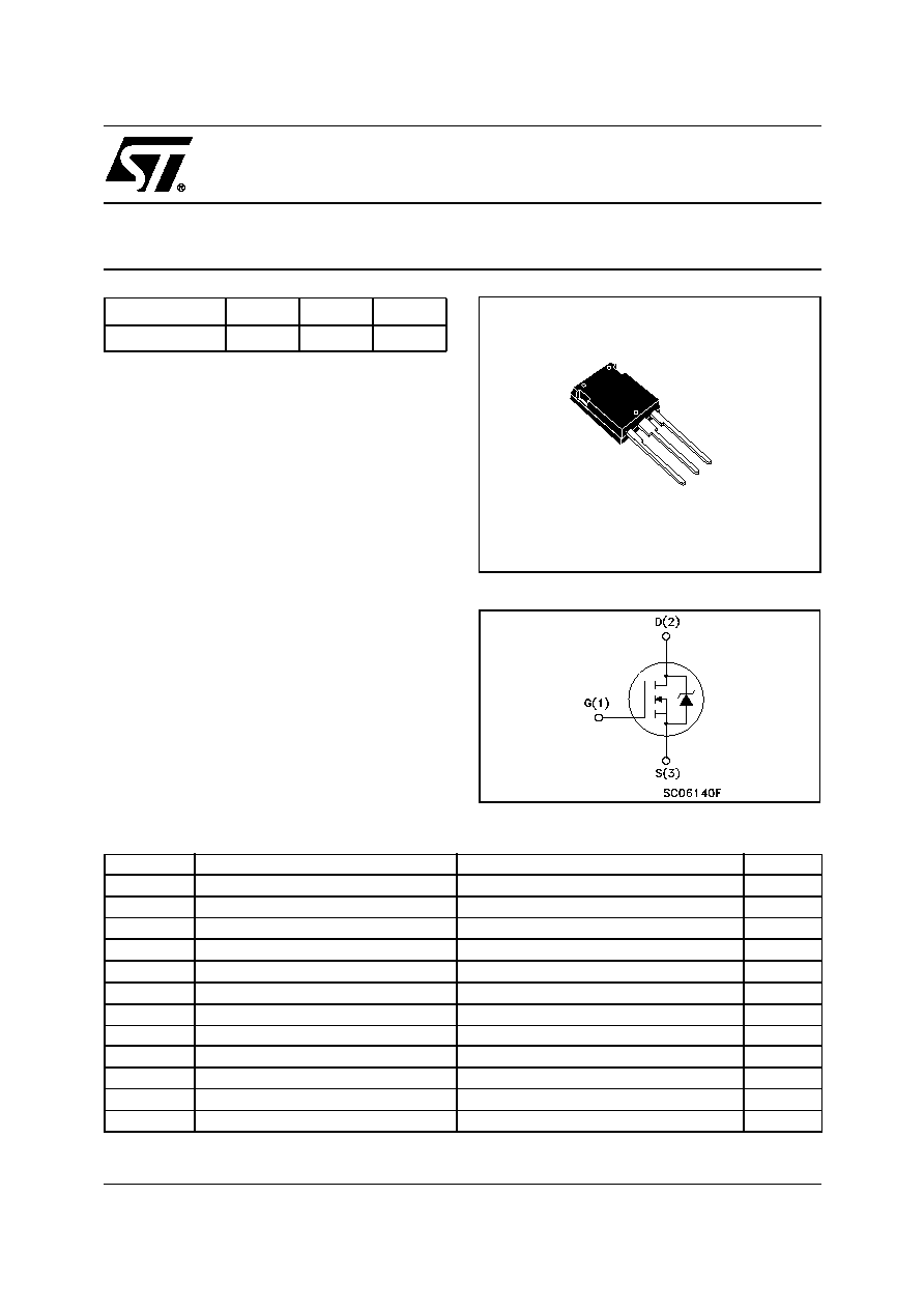
STY140NS10
N-CHANNEL 100V - 0.009
- 140A MAX247TM
MESH OVERLAYTM POWER MOSFET
s
TYPICAL R
DS
(on) = 0.009
s
STANDARD THRESHOLD DRIVE
s
100% AVALANCHE TESTED
DESCRIPTION
Using the latest high voltage MESH OVERLAYTM
process, STMicroelectronics has designed an advanced
family of power MOSFETs with outstanding
performances. The new patent pending strip layout
coupled with the Company's proprietary edge termination
structure, gives the lowest RDS(on) per area,
exceptional avalanche and dv/dt capabilities and
unrivalled gate charge and switching characteristics.
APPLICATIONS
s
HIGH CURRENT, HIGH SWITCHING SPEED
s
SWITCH MODE POWER SUPPLY (SMPS)
TYPE
V
DSS
R
DS(on)
I
D
STY140NS10
100V
<0.011
140A
1
2
3
Max247
TM
ABSOLUTE MAXIMUM RATINGS
(
∑)
Pulse width limited by safe operating area.
(1) Starting T
j
= 25
o
C, I
D
= 70A, V
DD
= 50V
(2) I
SD
140A, di/dt
200A/µs, V
DD
V
(BR)DSS
, T
j
T
JMAX.
Symbol
Parameter
Value
Unit
V
DS
Drain-source Voltage (V
GS
= 0)
100
V
V
DGR
Drain-gate Voltage (R
GS
= 20 k
)
100
V
V
GS
Gate- source Voltage
± 20
V
I
D
Drain Current (continuos) at T
C
= 25∞C
140
A
I
D
Drain Current (continuos) at T
C
= 100∞C
99
A
I
DM
(
∑)
Drain Current (pulsed)
560
A
P
tot
Total Dissipation at T
C
= 25∞C
450
W
Derating Factor
3
W/∞C
E
AS
(1)
Single Pulse Avalanche Energy
2900
mJ
dv/dt
(2)
Peak Diode Recovery voltage slope
5
V/ns
T
stg
Storage Temperature
-55 to 175
∞C
T
j
Operating Junction Temperature
-55 to 175
∞C
INTERNAL SCHEMATIC DIAGRAM
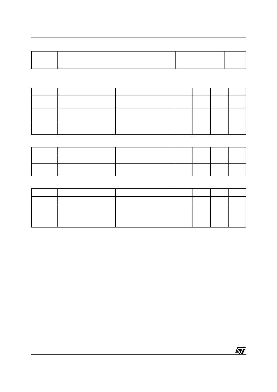
STY140NS10
2/8
THERMAL DATA
ELECTRICAL CHARACTERISTICS (T
case
= 25 ∞C unless otherwise specified)
OFF
ON
(1)
DYNAMIC
Rthj-case
Rthj-amb
T
j
Thermal Resistance Junction-case
Thermal Resistance Junction-ambient
Maximum Lead Temperature For Soldering Purpose
Max
Max
Typ
0.33
30
300
∞C/W
∞C/W
∞C
Symbol
Parameter
Test Conditions
Min.
Typ.
Max.
Unit
V
(BR)DSS
Drain-source Breakdown
Voltage
I
D
= 250 µA, V
GS
= 0
100
V
I
DSS
Zero Gate Voltage
Drain Current (V
GS
= 0)
V
DS
= Max Rating
V
DS
= Max Rating T
C
= 125∞C
1
10
µA
µA
I
GSS
Gate-body Leakage
Current (V
DS
= 0)
V
GS
= ± 20V
±100
nA
Symbol
Parameter
Test Conditions
Min.
Typ.
Max.
Unit
V
GS(th)
Gate Threshold Voltage
V
DS
= V
GS
I
D
= 250 µA
2
4
V
R
DS(on)
Static Drain-source On
Resistance
V
GS
= 10 V
I
D
= 70 A
0.009
0.011
Symbol
Parameter
Test Conditions
Min.
Typ.
Max.
Unit
g
fs (*)
Forward Transconductance
V
DS
= 20 V
I
D
= 70 A
50
S
C
iss
C
oss
C
rss
Input Capacitance
Output Capacitance
Reverse Transfer
Capacitance
V
DS
= 25V, f = 1 MHz, V
GS
= 0
12600
2100
690
pF
pF
pF

3/8
STY140NS10
SWITCHING ON
SWITCHING OFF
SOURCE DRAIN DIODE
(*)
Pulsed: Pulse duration = 300 µs, duty cycle 1.5 %.
(
∑)
Pulse width limited by safe operating area.
Symbol
Parameter
Test Conditions
Min.
Typ.
Max.
Unit
t
d(on)
t
r
Turn-on Delay Time
Rise Time
V
DD
= 50 V
I
D
= 70 A
R
G
= 4.7
V
GS
= 10 V
(Resistive Load, Figure 1)
40
150
ns
ns
Q
g
Q
gs
Q
gd
Total Gate Charge
Gate-Source Charge
Gate-Drain Charge
V
DD
=50V I
D
=140A V
GS
=10V
(see test circuit, Figure 2)
450
70
170
600
nC
nC
nC
Symbol
Parameter
Test Conditions
Min.
Typ.
Max.
Unit
t
d(off)
t
f
Turn-off Delay Time
Fall Time
V
DD
= 50 V
I
D
= 70 A
R
G
= 4.7
,
V
GS
= 10 V
(Resistive Load, Figure 1)
465
270
ns
ns
Symbol
Parameter
Test Conditions
Min.
Typ.
Max.
Unit
I
SD
I
SDM
(
∑
)
Source-drain Current
Source-drain Current (pulsed)
140
560
A
A
V
SD
(*)
Forward On Voltage
I
SD
= 140 A
V
GS
= 0
1.5
V
t
rr
Q
rr
I
RRM
Reverse Recovery Time
Reverse Recovery Charge
Reverse Recovery Current
I
SD
= 140 A
di/dt = 100A/µs
V
r
= 20 V
T
j
= 150∞C
(Inductive Load, Figure 3)
275
2
15
ns
µ
C
A
ELECTRICAL CHARACTERISTICS (continued)
Safe Operating Area
Thermal Impedance

STY140NS10
4/8
Output Characteristics
Transfer Characteristics
Transconductance
Static Drain-source On Resistance
Gate Charge vs Gate-source Voltage
Capacitance Variations

5/8
STY140NS10
Normalized Gate Threshold Voltage vs Temperature
Normalized on Resistance vs Temperature
Source-drain Diode Forward Characteristics
Normalized Breakdown Voltage vs Temperature
.
.