 | –≠–ª–µ–∫—Ç—Ä–æ–Ω–Ω—ã–π –∫–æ–º–ø–æ–Ω–µ–Ω—Ç: STY34NB50 | –°–∫–∞—á–∞—Ç—å:  PDF PDF  ZIP ZIP |

STY34NB50
N - CHANNEL 500V - 0.11
- 34 A - Max247
PowerMESH
TM
MOSFET
s
TYPICAL R
DS(on)
= 0.11
s
EXTREMELY HIGH dv/dt CAPABILITY
s
±
30V GATE TO SOURCE VOLTAGE RATING
s
100% AVALANCHE TESTED
s
LOW INTRINSIC CAPACITANCE
s
GATE CHARGE MINIMIZED
s
REDUCED VOLTAGE SPREAD
DESCRIPTION
Using the latest high voltage MESH OVERLAY
TM
process, SGS-Thomson has designed an ad-
vanced family of power MOSFETs with outstand-
ing performances. The new patent pending strip
layout coupled with the Company's proprietary
edge termination structure, gives the lowest
RDS(on) per area, exceptional avalanche and
dv/dt capabilities and unrivalled gate charge and
switching characteristics.
APPLICATIONS
s
HIGH CURRENT, HIGH SPEED SWITCHING
s
SWITCH MODE POWER SUPPLY (SMPS)
s
DC-AC CONVERTER FOR WELDING
EQUIPMENT AND UNINTERRUPTABLE
POWER SUPPLY AND MOTOR DRIVE
Æ
INTERNAL SCHEMATIC DIAGRAM
June 1998
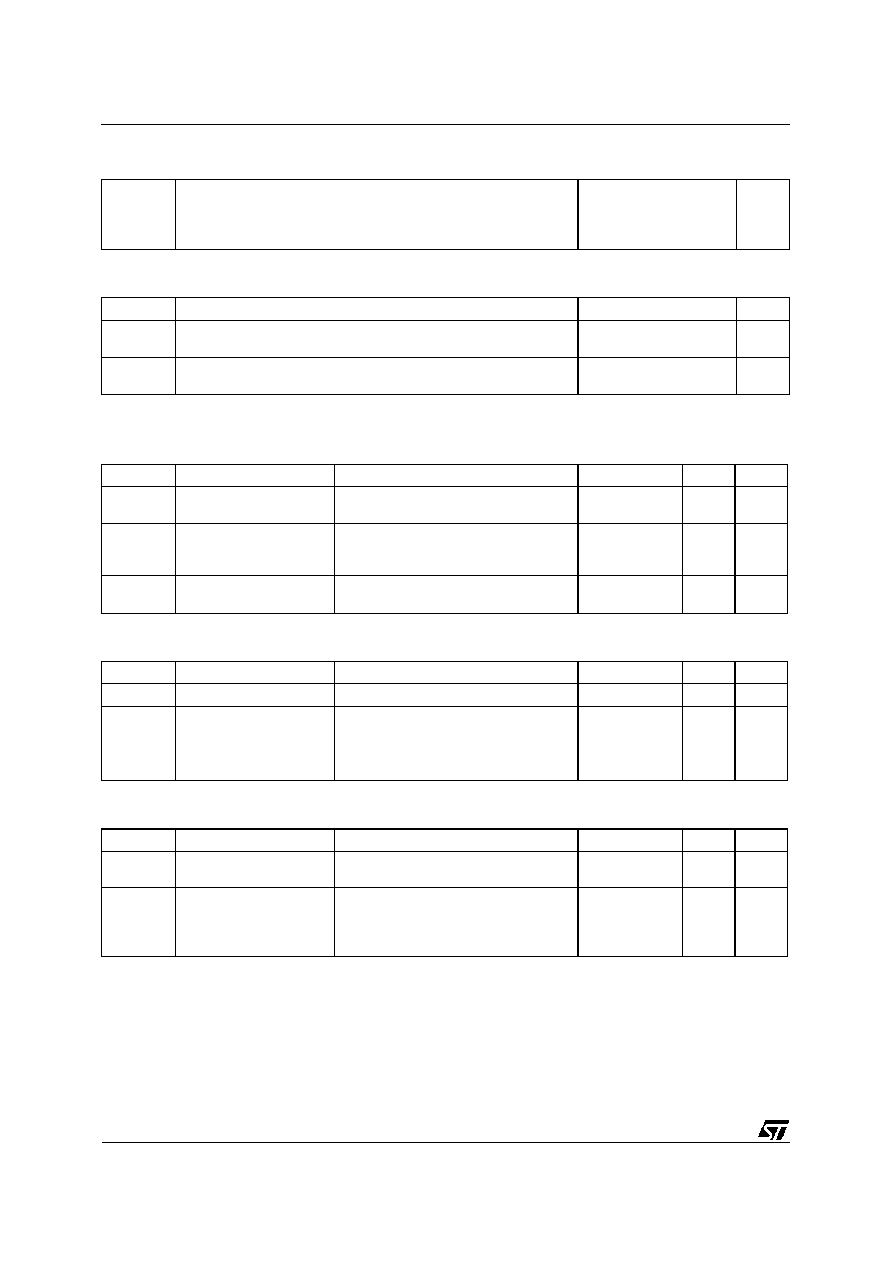
ABSOLUTE MAXIMUM RATINGS
Symbol
Parameter
Val ue
Uni t
V
DS
Drain-source Volt age (V
GS
= 0)
500
V
V
DGR
Drain- gat e Volt age (R
GS
= 20 k
)
500
V
V
GS
Gate-source Voltage
±
30
V
I
D
Drain Current (continuous) at T
c
= 25
o
C
34
A
I
D
Drain Current (continuous) at T
c
= 100
o
C
21. 4
A
I
DM
(
∑
)
Drain Current (pulsed)
136
A
P
t ot
Total Dissipation at T
c
= 25
o
C
450
W
Derat ing Factor
3. 61
W/
o
C
dv/dt
(1)
Peak Diode Recovery voltage slope
4.5
V/ ns
T
stg
St orage Temperature
-65 to 150
o
C
T
j
Max. Operating Junction T emperature
150
o
C
(
∑
) Pulse width limited by safe operating area
(
1
) I
SD
34 A, di/dt
200 A/
µ
s, V
DD
V
(BR)DSS
, T
j
T
JMAX
TYPE
V
DSS
R
DS(on)
I
D
ST Y34NB50
500 V
< 0.13
34 A
1
2
3
Max247
TM
1/8
THERMAL DATA
R
t hj-ca se
R
t hj- amb
R
thc- si nk
T
l
Thermal Resist ance Junction-case
Max
Thermal Resist ance Junction-ambient
Max
Thermal Resist ance Case-sink
Typ
Maximum Lead Temperature For Soldering Purpose
0. 277
30
0.1
300
o
C/W
o
C/W
o
C/W
o
C
AVALANCHE CHARACTERISTICS
Symb ol
Parameter
Max Valu e
Uni t
I
AR
Avalanche Current, Repetitive or Not -Repetitive
(pulse width limited by T
j
max)
34
A
E
AS
Single Pulse Avalanche Energy
(starting T
j
= 25
o
C, I
D
= I
AR
, V
DD
= 50 V)
1000
mJ
ELECTRICAL CHARACTERISTICS (T
case
= 25
o
C unless otherwise specified)
OFF
Symb ol
Parameter
Test Cond ition s
Mi n.
Typ .
Max.
Un it
V
(BR)DSS
Drain-source
Breakdown Volt age
I
D
= 250
µ
A
V
G S
= 0
500
V
I
DSS
Zero Gat e Voltage
Drain Current (V
GS
= 0)
V
DS
= Max Rating
V
DS
= Max Rating
T
c
= 125
o
C
10
100
µ
A
µ
A
I
GSS
Gate-body Leakage
Current (V
DS
= 0)
V
G S
=
±
30 V
±
100
nA
ON (
)
Symb ol
Parameter
Test Cond ition s
Mi n.
Typ .
Max.
Un it
V
GS(th)
Gate T hreshold Voltage V
DS
= V
GS
I
D
= 250
µ
A
3
4
5
V
R
DS( on)
St atic Drain-source O n
Resistance
V
G S
= 10 V
I
D
= 17 A
0. 11
0.13
I
D(o n)
On Stat e Drain Current
V
DS
> I
D(on)
x R
DS(on) max
V
G S
= 10 V
34
A
DYNAMIC
Symb ol
Parameter
Test Cond ition s
Mi n.
Typ .
Max.
Un it
g
fs
(
)
Forward
Transconductance
V
DS
> I
D(on)
x R
DS(on) max
I
D
= 17 A
18
20
S
C
iss
C
oss
C
rss
Input Capacitance
Output Capacit ance
Reverse Transfer
Capacitance
V
DS
= 25 V
f = 1 MHz
V
GS
= 0
7000
950
80
9100
1235
104
pF
pF
pF
STY34NB50
2/8

ELECTRICAL CHARACTERISTICS (continued)
SWITCHING ON
Symb ol
Parameter
Test Cond ition s
Mi n.
Typ .
Max.
Un it
t
d(on)
t
r
Turn-on T ime
Rise Time
V
DD
= 250 V
I
D
= 17 A
R
G
= 4.7
V
G S
= 10 V
(see t est circuit, f igure 3)
46
32
64
45
ns
ns
Q
g
Q
gs
Q
gd
Total G ate Charge
Gate-Source Charge
Gate-Drain Charge
V
DD
= 400 V I
D
= 34 A V
GS
= 10 V
159
35
67
223
nC
nC
nC
SWITCHING OFF
Symb ol
Parameter
Test Cond ition s
Mi n.
Typ .
Max.
Un it
t
r(Vof f)
t
f
t
c
Of f-voltage Rise Time
Fall Time
Cross-over T ime
V
DD
= 400 V
I
D
= 34 A
R
G
= 4.7
V
G S
= 10 V
(see t est circuit, f igure 5)
56
53
120
78
74
168
ns
ns
ns
SOURCE DRAIN DIODE
Symb ol
Parameter
Test Cond ition s
Mi n.
Typ .
Max.
Un it
I
SD
I
SDM
(
∑
)
Source-drain Current
Source-drain Current
(pulsed)
34
136
A
A
V
SD
(
)
Forward O n Volt age
I
SD
= 34 A
V
GS
= 0
1.6
V
t
rr
Q
rr
I
RRM
Reverse Recovery
Time
Reverse Recovery
Charge
Reverse Recovery
Current
I
SD
= 34 A
di/dt = 100 A/
µ
s
V
DD
= 100 V
T
j
= 150
o
C
(see t est circuit, f igure 5)
950
12
25
ns
µ
C
A
(
) Pulsed: Pulse duration = 300
µ
s, duty cycle 1.5 %
(
∑
) Pulse width limited by safe operating area
Safe Operating Area
Thermal Impedance
STY34NB50
3/8

Output Characteristics
Transconductance
Gate Charge vs Gate-source Voltage
Transfer Characteristics
Static Drain-source On Resistance
Capacitance Variations
STY34NB50
4/8

Normalized Gate Threshold Voltage vs
Temperature
Source-drain Diode Forward Characteristics
Normalized On Resistance vs Temperature
STY34NB50
5/8