 | ÐлекÑÑоннÑй компоненÑ: TDA7268 | СкаÑаÑÑ:  PDF PDF  ZIP ZIP |
Äîêóìåíòàöèÿ è îïèñàíèÿ www.docs.chipfind.ru
TDA7268
2 x 2W STEREO AUDIO AMPLIFIER
WIDE OPERATING RANGE FROM 4.5V TO 18V
P
OUT
= 2W @ THD 10% 12V/8
INTERNAL FIXED GAIN 32dB
NO FEEDBACK CAPACITOR
NO BOUCHEROT CELL
THERMAL PROTECTION
AC SHORT CIRCUIT PROTECTION
SVR CAPACITOR FOR BETTER RIPPLE
REJECTION
LOW TURN-ON/OFF POP
VERY FEW EXTERNAL COMPONENTS
STAND-BY MODE (I
ST-BY
< 300
µ
A)
DESCRIPTION
The device TDA7268 is a new technology stereo
Audio Amplifier in DIP package specially de-
signed for TV application.
Thanks to the fully complementary output configu-
ration the device delivers a rail to rail voltage
swing without need of boostrap capacitor.
March 1998
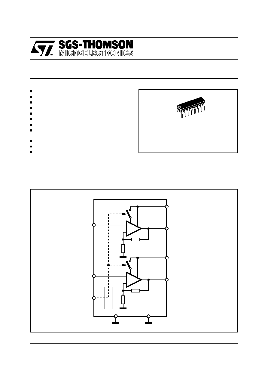
IN1
V
S1
OUT1
D94AU167B
IN2
SVR
S-GND
OUT2
P-GND
+
-
+
-
V
S2
1
4
2
8
7
5
3
6
9
÷
16
BLOCK DIAGRAM
ORDERING NUMBER: TDA7268
POWERDIP (8+8)
1/5
ABSOLUTE MAXIMUM RATINGS
Symbol
Parameter
Value
Unit
V
S
Operating Supply Voltage
18
V
I
O
Output Peak Current
1.5
A
T
op
Operating Temperature Range
0 to 70
°
C
T
j
Junction Temperature
150
°
C
T
stg
Storage Temperature Range
-40 to 125
°
C
THERMAL DATA
Symbol
Parameter
Value
Unit
R
th j-amb
Thermal Resistance Junction to ambient (on PCB) Max.
70
°
C/W
R
th j-case
Thermal Resistance Junction to case Max.
15
°
C/W
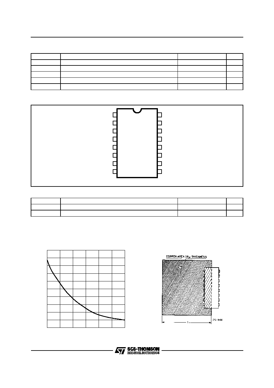
V
S1
OUT1
SVR
IN1
IN2
OUT2
S-GND
1
3
2
4
5
6
7
16
15
14
13
12
10
11
D94AU164A
V
S2
8
PGND
9
PGND
PGND
PGND
PGND
PGND
PGND
PGND
PIN CONNECTION
0
2
4
6
8
10
12
ON BOARD HEAT-SINK AREA (sq.cm)
THERMAL RESISTANCE JUNCTION TO AMBIENT(°C/W)
34
36
38
40
42
44
46
48
50
52
54
D98AU830
Rth with "on Board" Square Heat Sink vs. Copper
Area
Example of heatsink using PC board copper
TDA7268
2/5
ELECTRICAL CHARACTERISTICS (T
amb
= 25
°
C; V
S
= 12V; R
L
= 8
; f = 1KHz; unless otherwise specified.)
Symbol
Parameter
Test Condition
Min.
Typ.
Max.
Unit
V
S
Supply Voltage Range
4.5
18
V
I
S
Quiescent Current
40
60
mA
I
sb
Stand-By Current
Pin 3 shorted to GND
0.15
0.3
mA
V
O
Quiescent Output Voltage
5.5
6
6.5
V
A
V
Voltage Gain
31
32
33
dB
A
V
Voltage Gain Matching
1.0
dB
R
IN
Input Impedance
50
100
K
P
O
Output Power
THD = 10%
1.9
2
W
THD
Distortion
P
O
= 1W
0.1
0.4
%
SVR
Supply Voltage Rejection
V
rip.
= 150mVrms; F
rip.
= 1KHz
R
S
= 10k
R
S
= 50
40
50
46
dB
dB
e
n
Total Input Noise Voltage
Rg = 10K
; BW = 20Hz to
20KHz
4
8
µ
V
CT
Cross Talk
P
O
= 1W;
50
60
dB
V
sb
Stand-By Enable Voltage
I
SB
< 300
µ
A
1
V
A
sb
Stand-By Attenution
60
80
dB
P
O
Output Power
THD = 10%; V
S
= 9V; R
L
= 4
1.8
W
TDA7268
3/5
APPLICATION HINTS:
For 12V supply and 8
speaker application, its
maximum power dissipation is about 2W.
Assumming that max ambient temperature is
70
°
C. Required thermal resistance of the device
and heat dissipating means must be equal to (150
- 70)/2 = 40
°
C/W.
Junction to pin thermal resistance of the package
is about 15
°
C/W.
That means external heat sink of about 25
°
C/W is
required. Stand-By switches must be able to dis-
charge C
svr
current.
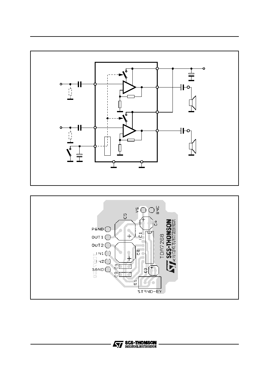
IN1
V
S1
OUT1
D94AU168D
IN2
SVR
S-GND
OUT2
P-GND
+
-
+
-
V
S2
C4
100
µ
F
V
S
=12V
C5
470
µ
F
8
IN1
C6 470
µ
F
8
C2 0.1
µ
F
C3
47
µ
F
IN2
C1 0.1
µ
F
S1
STAND-BY
1
4
2
8
7
5
3
6
9
÷
16
R1
10K
R2
10K
Note: Add R1 & R2 on demoboard only for DC tests.
Fig. 1: Standard Test and Application Circuit
Fig. 2: PCB And Components Layout Of The Application Circuit of Figure 1
TDA7268
4/5
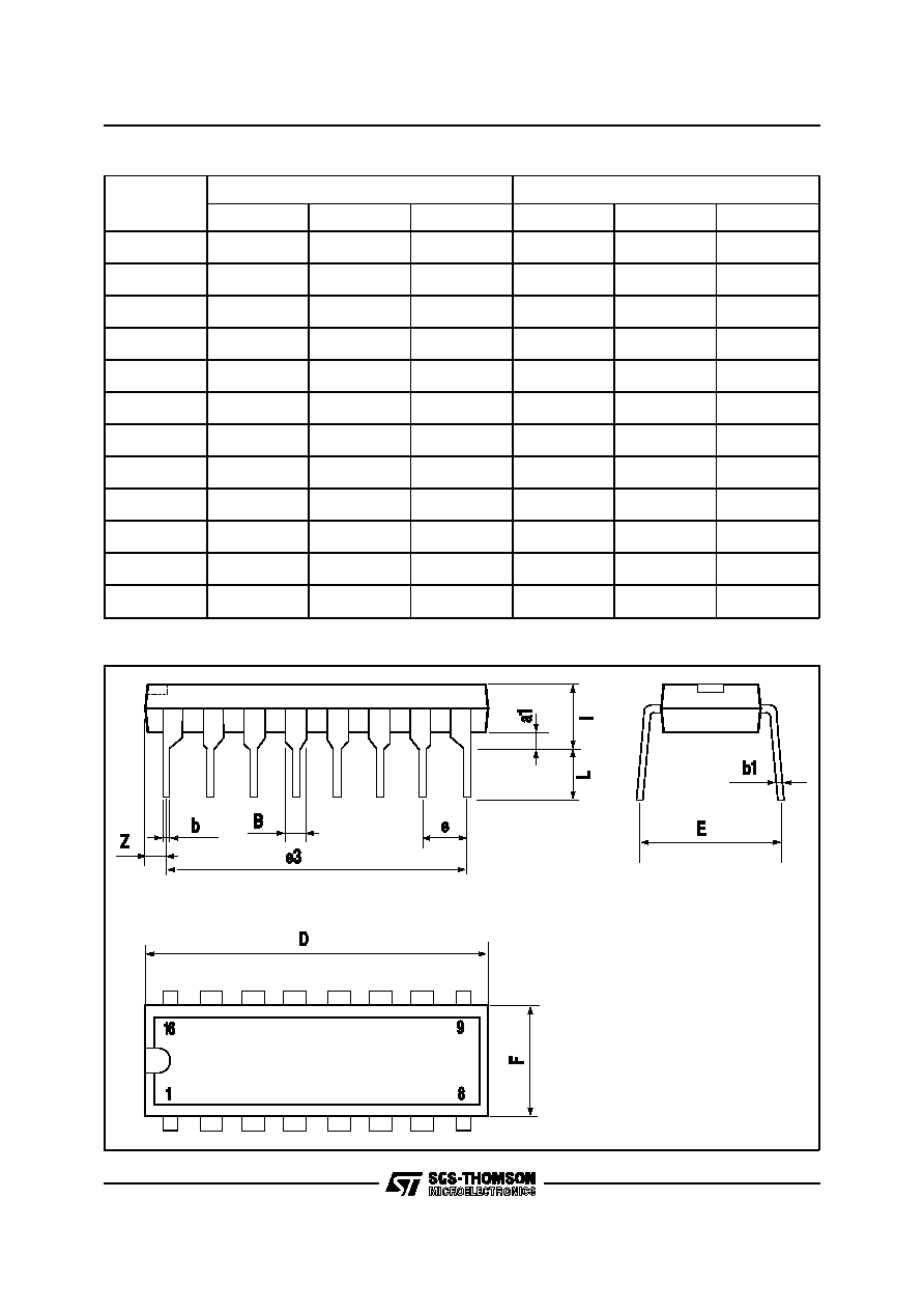
DIP16 PACKAGE MECHANICAL DATA
DIM.
mm
inch
MIN.
TYP.
MAX.
MIN.
TYP.
MAX.
a1
0.51
0.020
B
0.77
1.65
0.030
0.065
b
0.5
0.020
b1
0.25
0.010
D
20
0.787
E
8.5
0.335
e
2.54
0.100
e3
17.78
0.700
F
7.1
0.280
I
5.1
0.201
L
3.3
0.130
Z
1.27
0.050
TDA7268
5/5